
What is SMT PCBA?
SMT (Surface Mount Technology) PCBA (Printed Circuit Board Assembly) is the process of assembling electronic components onto a PCB (printed circuit board) using automated assembly techniques. In SMT manufacturing, components are mounted directly onto the surface of the PCB instead of through holes. This allows for smaller, more compact circuit designs.
Some key things to know about SMT PCBA:
- Components are mounted on the surface of the PCB using solder paste and then sent through a reflow oven to melt the solder and attach the components. This is faster than traditional through-hole assembly.
- Common component types used include capacitors, resistors, ICs, connectors, LEDs, etc.
- SMT components come in standardized packaging like SOIC, QFP, BGA for automated assembly.
- SMT allows for miniaturization and increased component density on a PCB.
- Requires specialized SMT equipment like pick and place machines, reflow ovens, AOI.
- Higher initial setup cost but reduced labor expenses compared to traditional PCB assembly.
SMT PCBA Process Step-by-Step
The typical SMT PCBA production process involves the following key steps:
1. SMT Stencil Printing
- A stencil is used to apply solder paste to the PCB pads.
- The stencil has cutouts matching the pad layout on the PCB.
- Solder paste is dispensed onto the stencil and a squeegee blade smears the paste across filling the stencil apertures.
- The stencil is then removed, leaving solder paste deposits on the PCB pads.
2. SMT Component Placement
- Components are placed onto the solder paste deposits.
- High-speed pick and place machines precisely place components onto the boards.
- Feeders containing reels, trays or sticks of components supply the pick and place machines.
3. Solder Reflow
- The PCB assemblies pass through a reflow oven with temperature profiles to melt the solder paste.
- The solder paste reflows forming solder joints that mount the components.
- Convection, vapor phase or infrared heating methods are used.
- Peak temperatures reach 230°C or higher for lead-free solder.
4. Automated Optical Inspection
- PCBs are inspected by automated optical inspection (AOI) machines.
- High-resolution cameras capture images to check for defects like missing or misaligned components.
- Helps catch defects early before further assembly steps.
5. Conformal Coating
- A protective plastic coating is often selectively applied to the PCB.
- The coating prevents environmental damage from moisture, dust, chemicals.
- Done by automated spraying machines.
- Areas like connectors may be masked off to avoid coating.
6. Program Loading/Functional Test
- For circuit boards with programmable components like microcontrollers, the firmware or software is loaded.
- Basic functionality testing may also be done.
- This may be done before and/or after conformal coating.
| SMT Process Step | Key Equipment Used |
|---|---|
| Solder Paste Printing | Stencil Printer |
| Component Placement | SMT Pick-and-Place Machine |
| Solder Reflow | Reflow Oven |
| Inspection | AOI Machine |
| Conformal Coating | Spray Equipment |
| Program Loading/Test | SMT Test Machines |
This covers the typical SMT PCBA production process from start to finish. There are many details and options within each step, but this provides an overview of the core manufacturing stages.
Advantages of SMT Assembly
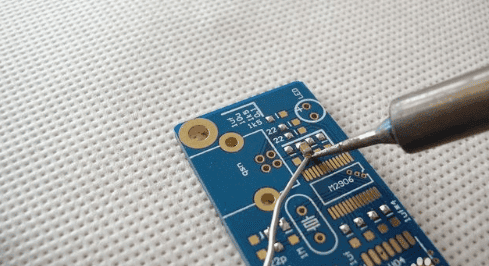
There are a number of important benefits that make SMT the preferred assembly method for modern PCB production:
- Miniaturization – SMT allows for much higher component density compared to through-hole assembly. Components can be as small as 0201 or 01005 size.
- Automation – SMT is highly automated with machines for each step reducing labor cost.
- Speed – Automated SMT lines have very fast throughput with some achieving over 35,000 components placed per hour.
- Quality – Machines produce consistent and high-quality solder joints. Automated inspection improves reliability.
- Flexibility – Quick changeovers between SMT component reels allows flexible productions of varying boards.
- Lead-Free Compatible – SMT process can handle the higher temperatures of lead-free soldering.
- Reduced Costs – Despite higher initial capital equipment costs, reduced labor expense makes SMT cost effective for medium to high volume production.
For these reasons, the vast majority of modern electronics manufacturing utilizes SMT assembly. As component sizes shrink and complexity increases, SMT allows efficient assembly of high-density PCBs.
Key Considerations for SMT PCBA
Here are some of the top considerations when planning your SMT PCBA manufacturing:
Component Selection
- Choose component packages designed for SMT like SOIC, QFP, BGA. Avoid through-hole parts when possible.
- Pay attention to component sizes with pitch and dimensions that work with your board layout rules.
- Select component thickness that is compatible with your PCB thickness.
Board Layout for SMT
- Use proper pad geometries for different component packages. Refer to IPC standards.
- Follow assembly clearances and spacing rules between components and pads.
- Use fiducials and component outlines for accurate automated placement.
- Minimize component height variations across the board. Select low profile components when available.
Solder Paste and Reflow Profile
- Use solder paste compatible with your PCB finish and solder masks. Match alloy composition.
- Optimize the reflow profile temperatures and times for your board and components.
- Consider factors like thermal mass, number of heat zones, and cooling rate.
Supplier Qualification
- Audit and qualify both your PCB and SMT assembly suppliers based on capabilities, quality, certifications, etc.
- Utilize suppliers capable of high-mix, low-volume prototype runs all the way to high-volume production.
- Validate required process capabilities like soldering for lead vs lead-free parts.
SMT PCBA Equipment Overview
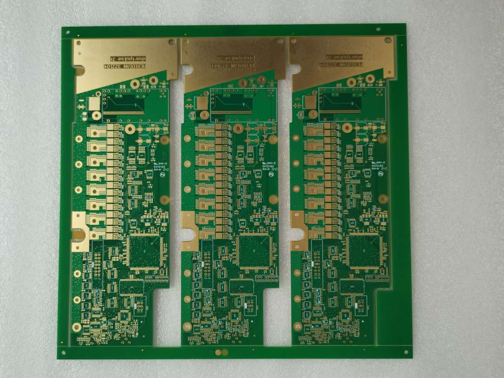
Specialized equipment is used in each stage of the SMT PCBA process:
Solder Paste Printing Equipment
- Stencil Printer – uses stencils to print precise amounts of solder paste onto PCB pads
- Solder Paste Inspection – checks volume and height of printed paste deposits
Component Placement
- SMT Pick-and-Place – automated machines to accurately pick components from reels/trays and place onto boards
- SMT Feeders – reel, stick and tray feeders hold and supply components to pick-and-place
Solder Reflow
- Reflow Oven – provides controlled heating profile to reflow (melt) solder paste
- In-line Reflow – conveyor based continuous process reflow oven
- Batch Reflow – reflow oven processes PCBs in batches
Inspection Equipment
- Automated Optical Inspection (AOI) – inspection of components post reflow using cameras
- Automated X-Ray Inspection (AXI) – x-ray imaging to check solder joints and BGA connections
- ICT Tester – checks for electrical shorts, opens, resistance, etc.
Software Tools
- SMT Line Management/MES – manages production scheduling, resource allocation, data collection
- SMT CAD and Documentation – generates assembly data likecentroid/pick-and-place files
SMT PCBA Defects and Troubleshooting
Some common SMT assembly defects, causes, and troubleshooting approaches:
| Defect | Potential Causes | Troubleshooting Approach |
|---|---|---|
| Tombstoning | Unbalanced paste deposits, component pitch issues | Adjust stencil design, paste volume, component orientation |
| Solder Beads/Bridges | Excess paste volume, solder mask issues | Optimize stencil and pad design, adjust paste printing process |
| Solder Voids | Low paste volume, poor wetting, outgassing | Increase paste deposit volume, adjust reflow profile, use voiding package styles |
| Skewed Components | Uneven paste height, placement accuracy issues | Tunestencil/printer, optimize pick-and-place calibration |
| Solder Balls/Splatter | High paste volume, poor reflow profile | Adjust paste volume, reflow oven settings |
| Warped Boards | Thermal or moisture stresses | Optimize board layout, material selection, handling procedures |
Careful inspection both during and after assembly can help identify defects early. Cross-functional collaboration between design, fabrication, and assembly teams aids rapid diagnosis and correction of issues.
FAQ
What are some key specifications for SMT PCBA?
Some key specifications include:
- Pitch – spacing between pads/components
- Component size, height, and series
- PCB parameters like thickness and finish
- Solder paste alloy type (lead or lead-free)
- Resolution and accuracy of solder paste printing
- Placement accuracy of components
- Number of unique board types (low vs high mix)
- Layer count of PCBs
- Selective vs. full solder mask
What is the typical lead time for SMT PCBA production?
Lead times can range from 2 days for quick-turn prototypes up to 8+ weeks for complex, high-volume production. Typical lead times fall in the range of 1-4 weeks depending on factors like order quantity, manufacturing location, production schedule, procurement of components, etc.
What testing is performed for SMT PCBA?
Common testing includes:
- Visual inspection at multiple stages
- ICT electrical testing
- Boundary scan
- Functional validation testing
- Burn-in testing
- X-ray inspection
The specific testing methodology depends on the product requirements and industry.
What standards apply to SMT PCBA?
Key standards include:
- IPC standards like IPC-A-610 for Acceptability of Electronic Assemblies
- IPC-J-STD-001 Requirements for Soldered Electrical and Electronic Assemblies
- IPC-A-620 for cable and wire harness assemblies
- IPC 7711/7721 for rework and repair
- ISO 9001 Quality Management Systems
How can you reduce costs for SMT PCBA?
Cost reduction strategies include:
- Designing for manufacturability and standard components
- Higher volume production with volume discounts
- Local sourcing of components
- Using consigned or excess component inventories
- Standardizing processes and reducing changeovers
- Testing optimization and elimination of non-value add tests
- Right-shoring manufacturing to optimal geographic location