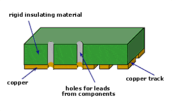
Surface mount technology (SMT) has revolutionized the electronics manufacturing industry. SMT enables the placement of electronic components directly onto the surface of printed circuit boards (PCBs), as opposed to through-hole technology where components have leads that are inserted into holes drilled in the PCB. This article provides an overview of SMT assembly, including key terminology, components, processes, equipment, challenges, and FAQs.
What is SMT Assembly?
SMT assembly, also known as SMT placement or SMT population, refers to the process of mounting and securing electronic components onto the surface of a PCB. The components, known as surface mount devices (SMDs), do not have wire leads but instead have small metallic pads that make electrical contact with the copper traces on the PCB when soldered into place.
The assembly process involves:
- SMD preparation
- Solder paste application
- SMD placement
- Soldering to attach components
- Cleaning and inspection
Well-designed SMT assembly results in smaller, lighter, and more reliable PCBs compared to through-hole assembly. SMT enables miniaturization and increased component density for modern electronic products.
SMT Components
Common types of SMT components include:
- Resistors and capacitors – Chip components up to about 1.5mm long. Available in a variety of case sizes.
- Inductors and transformers – Wound components with no leads. Ranges from 2mm to larger shielded power inductors.
- Integrated circuits (ICs) – Includes active components like microprocessors. Packages range from small quad flat packs (QFP) to large ball grid arrays (BGAs).
- Connectors – High density SMT connectors available. Some through hole connectors are transitioning to SMT.
- LEDs – Light emitting diodes used for illumination and displays. Very small SMT LEDs are widely used.
SMT Assembly Process Overview

The main steps in SMT assembly are:
SMD Storage and Kitting
SMDs are stored in temperature/humidity controlled stockrooms. They are pre-packaged into reels, trays, sticks, and tubes according to the component size and type. SMDs required for a particular PCB assembly are kitted or pulled together to deliver to the production line.
Solder Paste Application
Solder paste is a mixture of tiny solder particles and flux suspended in a thick medium. It is applied on PCB pads through screen printing, stenciling, or jet printing to provide adhesive and metallurgical bonding.
SMD Pick and Place
SMDs are precisely placed onto the solder paste deposits using high speed pick and place machines. Feeders or tapes position the components which are picked up by vacuum nozzles and placed on the PCB at extremely high speeds.
Solder Reflow
The PCB assemblies pass through soldering ovens which heat up to reflow and solidify the solder joints attaching the SMDs. Different solder alloys with specific melting points are used.
Cleaning and Inspection
Any residual flux or other contamination is removed from the soldered assemblies using cleaning processes. Automated optical inspection checks for any missing, misaligned or defective component placements.
SMT Equipment
Specialized equipment used in SMT production includes:
- Solder paste printers – Apply an even layer of solder paste on PCB pads.
- Pick and place machines – Automated SMD handling and high speed precise placement.
- Reflow ovens – Heat profiles reflow solder to form reliable solder joints.
- Inspection systems – Automated optical, x-ray, and in-circuit testers.
- Board handling – Conveyorized systems to move PCBs through process steps.
Challenges in SMT Assembly
Some challenges faced in SMT assembly include:
- Miniaturized components prone to handling damage.
- Dense component placement requires highly accurate pick-and-place machines.
- Fine pitch components need precise solder paste printing.
- Small solder joint sizes call for close process controls.
- Mix of large and small components on same board.
- Press fit connectors need controlled insertion force.
- Rework difficulties compared to through-hole components.
However, continued improvements in SMT equipment, soldering materials, component packaging, and assembly processes are overcoming these assembly challenges.
FAQs
Q: What are the benefits of SMT over through hole PCB assembly?
A: Key benefits include:
- Smaller PCB footprint leading to miniaturized electronics
- Higher component density enabling greater functionality
- Elimination of drilling provides flexibility in component placement
- Generally lower assembly costs at higher production volumes
- Typically faster assembly process and throughput
- Improved reliability with no leads to disconnect or break
Q: What size components are used in SMT?
A: The component package size typically ranges from 01005 chips of 0.4mm x 0.2mm up to 50mm x 50mm or larger ball grid array packages. 0201 (0.6mm x 0.3mm) and 0402 (1mm x 0.5mm) chip components are common.
Q: What types of solder paste are used?
A: Solder paste consists of spherical solder alloy particles suspended in a flux medium. Common solder alloys are SAC305 (tin, silver, copper) and Sn63Pb37. Flux allows solder wetting and protects against oxidation. No-clean and water soluble flux types are used.

Q: What factors affect solder paste printing quality?
A: Stencil design, aperture opening accuracy, stencil foil cut quality, stencil tensioning, printer setup, paste type, and cleaning maintenance all impact solder paste deposit consistency, thickness, and location. Automated optical inspection of prints is recommended.
Q: Does SMT assembly require a cleanroom environment?
A: Cleanliness standards ranging from ISO 14644-1 Class 8 to Class 4 are typically used depending on product type. Critical applications require tighter controls on temperature, humidity, and room cleanliness.
This overview covers the major aspects of surface mount technology PCB assembly. SMT has enabled the automated manufacturing of miniaturized, complex, and highly functional electronic circuit boards. Continued advances promise even smaller, faster, and lower cost SMT assembly.


0 Comments