A “footprint” in printed circuit board design refers to the pattern of copper pads, lines, and holes defining the area where a component connects onto a PCB. Like a human footprint pressed into sand, this imprint outlines the physical interface bridging components to circuit boards. Standardized footprints allow reliable assembly using compatible parts.
PCB footprints precisely match component packaging specifications so leads and pins align correctly with the solderable metal during fabrication. Accurate footprints ensure manufacturing assembly and reliability of circuit card designs. Without properly sized and located pad interfaces, boards malfunction or fail inspection.
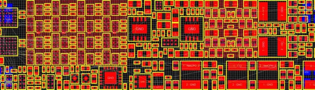
We explore what PCB footprints entail for common component types along with considerations translating packages into a connective layout footprint ready for fabrication and component mating during assembly.
Composition of Footprint Elements
PCB footprints interpret physical package properties like lead pitches, sizes, and termination interfaces into a series of drafted artwork features to locate active areas, pins, and construct attachment joints. This converts device properties into connective surface mount or through-hole features on boards.
Primary elements in a footprint include:
Pads
Metalized circular areas defining component pin connection points of a specific diameter and land size selected to ensure reliable solder joints based on package pin geometry and characteristics. They anchor device pins. Round, oval, or shaped cutouts surmounting holes serve through-hole pins.
Landing Patterns
Groups of pads arranged matching the configurations of component leads or connectors establish surface mounting anchor points. The pattern “lands” devices onto board layers. Phased pad arrays support self-alignment in reflow process.
Holes
Drilled circular openings allowing insertion of component leads to pass through boards entirely and get solder wicked on backside pads, forming a through-hole solder anchor. Flatted ends prevent leads rotating. Hole sizes support leads.
Lines
Thin drafted metal traces connecting pads to complete electrical connectivity from pins to internal routing layers of boards. Their widths depend on current levels. Lines also bridge isolated pads forming interfaces.
Silkscreen Outline
A visible perimeter line, usually on the top side, bounds footprint extent. It can reference part numbers or component designators for pick-n-place machine recognition during assembly to avoid misplacements.
Together, carefully sized and positioned pads, holes, lines and outlines create interface patterns between devices and board layers that constitute a component footprint specification.
Symbol View vs. PCB Layout Footprint View
Electronic schematic tools utilize a simplified “symbol” view of components to enable rapid circuit diagramming, while PCB layout environments use the full packaging-derived “footprint” implementation for fabrication. This symbol-to-footprint abstraction decouples logical connectivity planning from physical equivalents.
Symbol Views
Schematic symbols distill components down to logical pins and blocks representing fundamental electrical connectivity interfaces. A resistor symbol has just two pin attachments. No packaging represented. Symbols stay idealized.
PCB Footprints
Actual transformations of symbols into manufacturable footprint geometries adds physical constraints imposed by components and production – minimum line widths, terminal arrangements, etc. This grounds designs in reality.
Converting schematic symbols into layout footprints requires packaging-aware detailing while maintaining pin-mapping and net associations between domains. Libraries encode compatibility.
Footprint Categories
Major classes of PCB footprints fall into surface-mount or through-hole styles depending on component packaging technologies. Each has distinct attributes.
Surface Mount Footprints
Components soldering onto board surface layers use an underlying pattern of flat contact pads matching the lead terminal geometry protruding from device packages. Common surface mount types include:
Quad Flat Packages (QFP): Perimeter pins extending in a girdle pattern beneath rectangular molded plastic or ceramic IC bodies with pin pitch ranging 0.4mm to 1.0mm. High I/O capability.
Ball Grid Arrays (BGA): Input/output solder balls arranged in full grid matrices across bottom of square/rectangular devices requiring X-ray inspection after soldering for hidden joints beneath body. Pitch can reach 1.0mm.
Land Grid Array (LGA): Exposed copper pad arrays mate under devices with clamping mechanical pressure rather than solder to create electrical contact. Allow rework and socketing but less rugged.
Small Outline Integrated Circuits (SOIC): Narrow rectangular body with peripheral leads protruding from longer side intended for automated assembly. Versatile and inexpensive.
Through-hole Footprints
Leaded components passing conductors vertically through boards utilize pad/hole combinations. Some examples:
Dual In-line Package (DIP): Dual parallel rows of through-hole pins extending from long narrow IC body. Breadboard friendly but outdated. Pitch between lead rows rarely under 2.0mm.
Pin Grid Array (PGA): Dense rectangular grid of square pins underneath large ICs designed for sockets rather than soldering providing high I/O density at 1.27mm pitch or less.
Connector: Component joining external cables/wires utilize arrays of through-hole anchors for screw terminals, edge fingers, or wire crimp slots. Polarizing features prevent misalignments.
PCB Layout and Manufacturing Adjustments
To shift footprint concepts into physical board implementations involves adding dimensional clearances assisting fabrication and assembly processes:
Annular Rings
Soldermask openings called annular rings or lands surround pads exposed for mounting surface mount parts. The areas allow paste printing and ensure adequate fillets clinch components.
Thermal Reliefs
Truncated spokes called thermal reliefs radiating from plane layers reduce heat sinking allowing solder joints solidifying faster and evenly during reflow while hindering excess solder wicking.
Solder Mask Expansions
Additional soldermask clearance added around copper pad perimeters prevents paste bridging between neighboring joints even with slight mounting misalignments.
Accommodations transform ideal footprints into manufacturable interfaces tolerating real-world conditions. Libraries encode these rules.
Footprint Dimension Sources
To properly size PCB footprints requires referencing manufacturer package drawings or component datasheets for critical dimensions. Common attributes include:
Lead Width/Diameter
Soldering surface width on terminals determines minimum pad sizes for adherence. Excess pad area wicks more solder. Insufficient width risks open joints or tombstoning.
Row/Grid Spacing
Center-to-center distance between adjacent pad rows or grid arrays dictates landing pattern spacing. Loose arrays complicate assembly. Overly tight risks bridging.
Package Body Size
Component molded enclosure X/Y profile helps orient part visually. Size factors into spacing adjacent boards during panelizing also.
Lead/Pin Lengths
Maximum protrusion distance below package sets minimum clearance needed between bottom terminals and board to prevent shorting in tilt situations post soldering before full encapsulation.
Component models, recommendations from application notes, and prior platform precedence steer initial footprint sizing validations. Test boards confirm fit. Libraries adopt common footprints once proven to enable reuse.
Creating New PCB Footprints

For every new component package variant considered across the breadth of PCB designs, creating first-time matching footprints expands libraries enabling broader usage. Steps include:
1. Review Component Data
Gather all interface specifications – connector tables, ball grid spacing, pin locations, etc. Identify critical pins for orientation.
2. Sketch Draft Footprint
Layout approximate pad geometries scaled against dimensions with appropriate spacing and polarity indicators based on data gathered.
3. Implement in CAD System
Enter the preliminary footprint into PCB library editors, connecting all pins/pads with naming/numbering and setting initial text settings.
4. Validate Properties
Run design rule checks in PCB systems to confirm suitable spacing/overlap avoidance given acceptable board fabrication tolerances between features. Tweak as needed iteratively to pass geometry analysis cleanly.
5. Test On Prototype Boards
Fabricate simple breakout boards with part soldered validating assembly integrity and confirming no hidden violations cropped up affecting manufacturability. Finalize if passing prototype validations.
While can take effort ramping up new components initially, capturing proven reliable packages into company footprint libraries streamlines downstream designs leveraging past efforts reused.
PCB Footprint Design Guidelines
Certain guiding principles underpin effective footprint implementations balancing manufacturability needs:
Simplicity
The best footprints use the simplest grouping of pads/lines to appropriately interface devices while maximizing soldering surface areas for stronger joints and accommodating tolerances.
Clarity
Group pads belonging to common leads to aid human inspection. Clearly associate any split/mirrored differential pad groupings.
Labeling
Adding component designators as text labels or silkscreen parts outline helps assembly operators correctly place small devices by matching shapes and marking codes.
Standardization
Consistently implemented footprints using named geometry constructs, unified rules and common pad arrangements simplify maintenance integrating improvements or porting into alternative tools.
Adhering footprint designs focusing on fundamentals aids inspectability accommodating real-world considerations during fabrication and assembly for proven product outcomes.
Simulating Assembly Fit
With footprints modeled into CAD libraries, we can perform virtual test fittings assessing the viability of component selection paired against particular products under development. Steps include:
Obtaining Accurate 3D Package Models
Secure step model representations for all major IC/device selections to evaluate. Component vendors or online electronics CAD model marketplaces offer 3D body geometries.
Import Models Into MCAD Assembly
Bring package models into mechanical CAD environments alongside product enclosure models containing the PCB to virtually mock-up system fit.
Checking Keepouts
Move components around checking for collisions or tight fits indicating the combinations exceed spatial budgets. Watch for corner case orientations. Revise if needed.
Overlay PCB Layout
Import the board layout file and toggle component outlines opaque to view footprint interfaces align underneath models, confirming enough clearance from enclosure walls or internal device heights sitting over boards.
This realistic modeling exercise reveals limiting factors impacting hardware integration feasibility earlier compared to discovering issues once prototypes get ordered. Virtual system mockups assess complex edge cases.
PCB Footprint Management Practices
Including the right variety and versions of component footprints enables successful population of boards during fabrication assembly. Strategies managing PCB libraries involve:
Standards Compliance – Utilize proven industry-standard joint profiles standardized by IPC specifications based on component sizes and pin counts promoting interoperability. Follow guidelines on naming, geometry and spacing rules.
Release Process – Govern edits to footprint database by a formal release procedure ensuring changes tested on simple breakout boards first validating manufacturability before appearing on complex designs.
Lifecycle Control – Move superseded footprints into archived status if packaging evolves over component generations to prevent inadvertent reintroduction of outdated variants.
Parameterized Templates – Generalized footprints employing rules-driven tables for pin counts and body sizes flexibly generate tailored variants avoiding redundant duplications.
Third Party Validation – Leverage qualified footprint distribution channels from leading CAD software partners to utilize industry best-practices. Review notification alerts when key parts gain updates.
Proactive footprint husbandry safeguards smooth procurement and assembly preventing scrambled reworks holding up programs if deficiencies emerge during later manufacturing stages.
The Impact of Miniaturization
Electronics miniaturization shrinks component packages and condenses lead dimensions as newer chip technologies packing more capability into diminishing real estate emerge. This challenges PCB footprints accommodating such dense interfaces:
Pad/Line Scaling – Reduced pin widths/pitches mandate matching pad setbacks and trace geometries prevent shorting while retaining enough bonding surface area.
Fine Pitch Arrays – Grids with under 1mm pitch require shifting towards organic substrate boards offering tighter dimensional control or even employing laser direct structuring (LDS) additive patterning.
Alternate Attach – Extreme low profiles utilize non solder conductive glues or pressure mounting to overcome solder surface tension barriers.
Inspection Access – Micro BGA packages impede visual checks demanding intensified process controls combined with automated optical, x-ray or sonic examination tools verifying assembly integrity.
Adapting PCB construction enables translating even radically contracted component packages into functional interfaces interfacing next generation electronics into products.
Summary
In conclusion, PCB footprints provide the vital bridging artwork translating physical packaging dimensions and constraints into corresponding pad/hole arrangements supporting fabrication and assembly. Carefully crafted footprints:
- Match component lead spacing into board layers
- Factor in soldering clearances
- Utilize polarization indicators aiding human inspection
- Allow part dimension tracing clarifying datasheets
- Support best practices around simplicity and standardization
Getting footprints “right sized” for a given component and product build establishes the foundation enabling quality electronics manufacturing and by extension robust functioning end products.
Attention to properly capturing and documenting footprint design details pays dividends reducing ambiguities that undermine production outcomes for often intricate PCB constructions bridging elaborate electronics into pillar products.
Frequently Asked Questions
Here are answers to some common questions about PCB footprints:
Can I use the same PCB footprint for different components?
Sometimes if all interface dimensions and pins align. But differing component heights or attachment types often still require unique footprints tailored per part avoiding assembly issues. Review all specs first before assuming interchangeability.
What are common naming conventions used for PCB footprint filenames?
Standardized numbering schemes denoting package style, dimensions, pin counts (i.e. SOIC_7.5mm_16Pin) help organize libraries. Codes mapping to manufacturer conventions also aid identifying components during placement programming too.
What causes tombstoning defects during PCB assembly?
Insufficient pad area on one end of an offset component leads more rapidly heating causing that end to float upwards as solder liquefies before other side fully reflows. Widening pad sizes evenly prevents the imbalanced wicking.
Can PCB assembly machines place components on any footprint orientation?
Systems can rotate parts in 90 or 180 degree flipped alignments. But asymmetry may require squared-off alignment indicators on footprints ensuring proper positioning for polarized devices. Fiducials give additional mounting references.
What information should I provide PCB fabricators regarding footprints?
Supply complete packaged component data models, recommended footprints list with dimensions, and the target IPC land size standard used for your boards ensuring your fabrication partner understands assumptions made around interfaces.


0 Comments