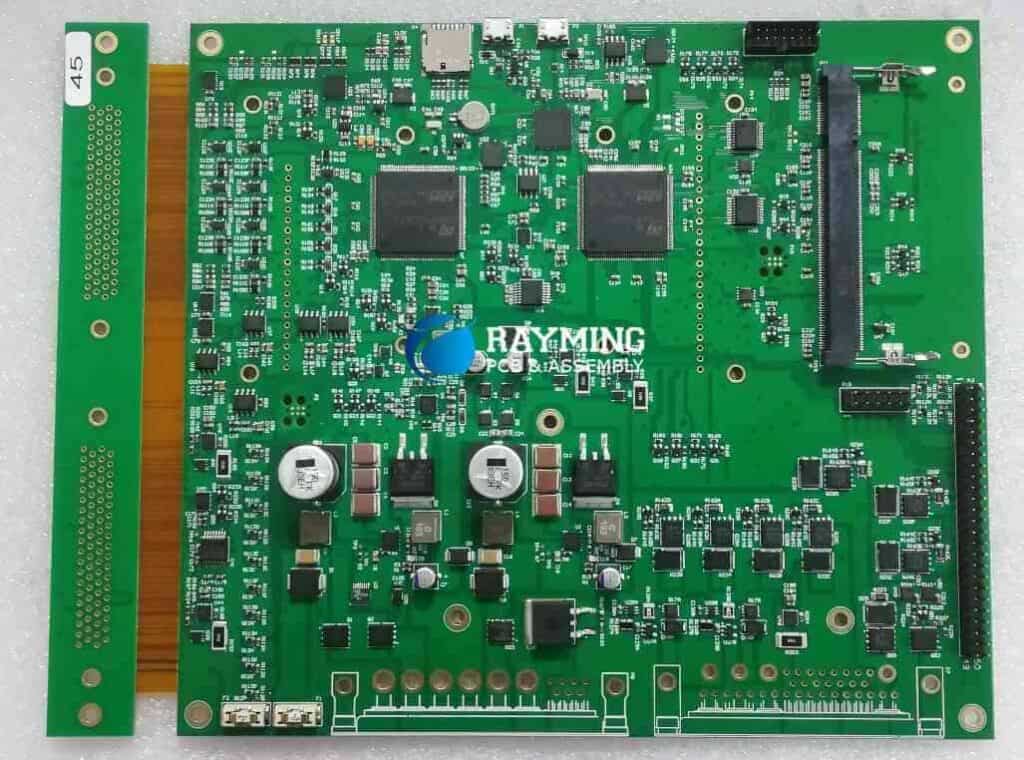
In the world of printed circuit board (PCB) design and manufacturing, silkscreen is a crucial element that aids in the identification, labeling, and visual representation of various components and features. Silkscreen, also known as legend printing or nomenclature, is a printing process that involves transferring ink or epoxy onto the surface of the PCB, creating high-contrast markings and text.
Silkscreen plays a vital role in enhancing the readability, organization, and overall functionality of PCBs, making it an essential aspect of both prototype and production boards. This comprehensive article will explore the intricacies of silkscreen on PCBs, including its purposes, materials, application techniques, design considerations, and best practices.
Purposes of Silkscreen on PCBs
Silkscreen serves several important purposes in PCB design and manufacturing:
- Component Identification: Silkscreen markings are used to label individual components on the PCB, such as integrated circuits (ICs), resistors, capacitors, and connectors. These labels aid in component identification during assembly, testing, and maintenance processes.
- Pin and Pad Designation: Silkscreen is often used to mark pin numbers or pad designations for various components, facilitating proper component placement and connectivity during the assembly process.
- Board Orientation and Polarity: Silkscreen markings can indicate the correct orientation and polarity of components, ensuring proper installation and functionality.
- Test Points and Debugging: Silkscreen can be used to mark test points, jumpers, or other areas of interest on the PCB, assisting in debugging, testing, and troubleshooting processes.
- Branding and Aesthetics: Silkscreen can be used to apply logos, product names, or other branding elements to the PCB, enhancing its visual appeal and professional appearance.
- Safety and Compliance: In some cases, silkscreen may be used to display safety warnings, regulatory markings, or compliance information required by industry standards or regulations.
Materials and Application Techniques
The materials and techniques used for silkscreen on PCBs vary depending on the desired characteristics and production requirements.
Materials
- Epoxy-based Inks: Epoxy-based inks are commonly used for silkscreen on PCBs due to their durability, resistance to solvents and chemicals, and ability to withstand high temperatures during the soldering process.
- Polymer-based Inks: Polymer-based inks offer an alternative to epoxy-based inks, providing improved flexibility and resistance to cracking or peeling.
- Conductive Inks: In certain applications, conductive inks containing metal particles (e.g., silver, carbon) may be used for silkscreen, allowing the creation of conductive traces or markings on the PCB.
- Solder Mask: In some cases, the solder mask layer itself can be used for silkscreen markings, providing a more integrated approach.
Application Techniques
- Screen Printing: The traditional silkscreen printing method involves transferring ink through a patterned mesh or stencil onto the PCB surface using a squeegee.
- Inkjet Printing: Advancements in inkjet printing technology have made it possible to directly print silkscreen markings onto PCBs using specialized inks and printers.
- Laser Marking: Laser marking techniques can be used to etch or engrave silkscreen markings onto the PCB surface, offering high precision and durability.
- Pad Printing: Pad printing, also known as tampography, involves transferring ink from a cliché (etched image) onto the PCB surface using a silicon pad, allowing for intricate and high-quality markings.
Design Considerations
When designing silkscreen for PCBs, several factors must be taken into consideration to ensure readability, accuracy, and compliance with industry standards and manufacturing capabilities.
- Text Size and Font: Silkscreen text should be legible and follow recommended font sizes and styles based on industry guidelines or specific application requirements.
- Component Clearance: Adequate clearance must be maintained between silkscreen markings and components or pads to prevent interference or short circuits.
- Polarity and Orientation Indicators: Clear indicators for component polarity and orientation should be included in the silkscreen design to facilitate proper assembly and functionality.
- Test Point and Debugging Markings: Appropriate markings for test points, jumpers, or other areas of interest should be incorporated into the silkscreen design to aid in testing and debugging processes.
- Branding and Aesthetics: When including branding elements or logos in the silkscreen design, consideration should be given to their placement, size, and visual impact on the overall PCB appearance.
- Layer Alignment: In multi-layer PCBs, proper alignment and registration of silkscreen markings across different layers is crucial to ensure accurate component placement and overall board functionality.
- Design Rules and Standards: Silkscreen design should adhere to industry standards, such as IPC (Association Connecting Electronics Industries) guidelines, as well as any specific requirements or design rules set by the PCB manufacturer or end-user.
Advantages and Limitations
Silkscreen on PCBs offers several advantages but also has some limitations that should be considered.
Advantages
- Improved Readability and Identification: Silkscreen markings enhance the readability and identification of components, pin designations, and other features on the PCB, facilitating assembly, testing, and maintenance processes.
- Enhanced Aesthetics: Well-designed silkscreen can improve the overall aesthetic appeal of the PCB, contributing to a professional and visually appealing product.
- Durability: Silkscreen markings, when applied with appropriate materials and techniques, can withstand harsh environments, high temperatures, and various chemical exposures, ensuring long-lasting legibility.
- Branding and Customization: Silkscreen allows for the inclusion of branding elements, logos, and customized markings, enabling product differentiation and enhancing brand recognition.
Limitations
- Limited Resolution and Detail: Silkscreen printing has inherent limitations in terms of resolution and detail, which may not be suitable for extremely fine or intricate markings.
- Potential Misalignment: In multi-layer PCBs, misalignment of silkscreen markings across layers can occur, leading to inaccuracies or errors in component placement and functionality.
- Material Compatibility: Certain PCB materials or surface finishes may not be compatible with specific silkscreen inks or application techniques, potentially affecting adhesion or durability.
- Cost and Lead Time: Depending on the complexity of the silkscreen design and the manufacturing process, additional costs and lead times may be incurred compared to PCBs without silkscreen or with simpler markings.
Best Practices
To ensure optimal performance, readability, and compliance with industry standards, it is essential to follow best practices when implementing silkscreen on PCBs:
- Adhere to Industry Standards: Follow relevant industry standards and guidelines, such as IPC-A-600 or IPC-7351, for silkscreen design, materials, and application techniques.
- Collaborate with PCB Manufacturers: Work closely with PCB manufacturers to understand their capabilities, design rules, and recommended practices for silkscreen implementation.
- Prioritize Readability: Ensure that silkscreen markings are legible and easily identifiable, considering factors such as text size, font, and contrast.
- Maintain Clearances: Maintain adequate clearances between silkscreen markings and components, pads, or other features to prevent interference or short circuits.
- Utilize Design Rule Checking (DRC): Implement design rule checking tools to identify and resolve any potential issues or violations related to silkscreen design before manufacturing.
- Conduct Thorough Testing: Perform comprehensive testing and verification of silkscreen markings, including alignment, accuracy, and durability, to ensure compliance with requirements and specifications.
- Document and Revise: Maintain accurate documentation of silkscreen designs and revisions, facilitating version control and enabling easy updates or modifications as needed.
- Consider Alternative Marking Methods: Explore alternative marking methods, such as laser marking or pad printing, for applications with specific requirements or limitations related to silkscreen.
Frequently Asked Questions (FAQs)
- Can silkscreen markings be applied to both sides of a PCB? Yes, silkscreen markings can be applied to both the top and bottom sides of a PCB, enabling component identification and labeling on both surfaces.
- What is the typical color used for silkscreen on PCBs? The most common color used for silkscreen on PCBs is white, as it provides high contrast and visibility against the green or blue solder mask layer. However, other colors can also be used depending on specific requirements or branding needs.
- Can silkscreen markings be removed or modified after the PCB is manufactured? While it is possible to remove or modify silkscreen markings using mechanical or chemical methods, it is generally not recommended as it can compromise the integrity and functionality of the PCB. Any changes to silkscreen markings should be addressed through a design revision and a new PCB manufacturing cycle.
- How does silkscreen affect the overall cost of a PCB? Silkscreen can add a modest increase to the overall cost of a PCB, depending on the complexity of the design, the materials used, and the manufacturing process. However, the benefits of improved readability, identification, and branding often outweigh the additional cost.
- Are there any environmental considerations related to silkscreen on PCBs? Some silkscreen inks or materials may contain substances that are regulated or restricted due to environmental concerns. It is important to ensure compliance with relevant environmental regulations and consider eco-friendly alternatives when available.
Conclusion
Silkscreen on PCBs is a vital element that enhances readability, identification, and overall functionality. By providing clear markings for components, pin designations, test points, and branding elements, silkscreen plays a crucial role in facilitating assembly, testing, maintenance, and product recognition.
Understanding the purposes, materials, application techniques, design considerations, and best practices related to silkscreen is essential for PCB designers, manufacturers, and end-users alike. Adhering to industry standards, collaborating with PCB manufacturers, and prioritizing readability and accuracy are key to ensuring successful silkscreen implementation.
As technology continues to evolve, the demand for compact and high-density PCBs increases, making the role of silkscreen even more significant. Advancements in materials, printing techniques, and design tools will further enhance the capabilities and precision of silkscreen, enabling more intricate and visually appealing PCB designs.
Whether for prototyping, small-scale production, or large-scale manufacturing, silkscreen on PCBs remains an indispensable aspect, contributing to the overall quality, reliability, and professional appearance of electronic products.


0 Comments