Introduction
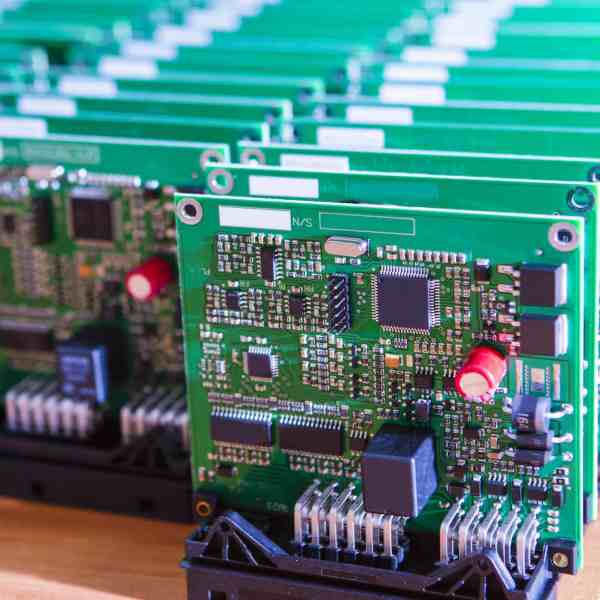
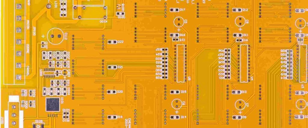
For engineers and designers developing new electronics hardware, having the ability to quickly turn around printed circuit board (PCB) prototypes is invaluable for accelerating project timelines. Quick turn PCBs allow validating designs and iterating faster.
This guide covers the key capabilities required for rapid PCB fabrication and assembly along with tips to optimize lead times.
Benefits of Quick Turn PCB Capabilities
Here are some of the major advantages of quick turn PCB production:
- Faster design validation – Verify schematics and layouts through prototyping.
- Accelerate time-to-market – Enable launching products faster.
- Rapid design iteration – Test multiple design variations quickly.
- Meet tight deadlines – Hit aggressive go-to-market targets.
- Stage gate efficiency – Transfer projects faster from development to production.
- Supplier flexibility – Make last minute component or fabrication changes.
For these reasons, the ability to get fast turn prototypes is highly useful during the new product introduction (NPI) phase.
Enablers of Quick Turn PCB Capabilities

To enable fast PCB fabrication and assembly, electronics partners need to have certain key capabilities:
PCB Fabrication
- Next day and 3-5 day fabrication options
- Optimized processes focused on speed
- Localized supply chain and production
- Priority scheduling for rush orders
- Engineering support for DFM
- Fast SMT pick-and-place equipment
- Local component inventory
- Parallel workflows and rapid processes
- Prioritized production scheduling -Accelerated test and inspection
- Shipping/logistics infrastructure
Evaluating partners on these parameters helps choose the ones most capable of meeting quick turn needs.
Key Design Considerations for Fast Prototype PCBs
To best leverage the capabilities of quick turn suppliers, engineers can optimize their PCB designs as follows:
- Use minimum layer counts (2-4 layer)
- Avoid high density interconnects
- Reduce board dimensions
- Standardize commonly used cells/blocks
- Utilize design for manufacturability practices
- Allow room for rework and modifications
- Add convenient test points
Keeping designs relatively simpler and more prototyping-friendly results in the fastest turnaround times.
Comparing Lead Times of Quick Turn Services
Here is a comparison of typical lead times offered for quick turn PCB production:
| Service | Standard Lead Time | Expedited Lead Time |
|---|---|---|
| PCB Fabrication | 4-5 days | 24-48 hours |
| PCB Assembly | 5-7 days | 3-5 days |
| Full Turnkey | 10-15 days | 5-7 days |
Note that expedited services usually have premium fees but offer significant time savings.
Domestic vs. Offshore Quick-Turn
Domestic PCB partners are best suited for extreme quick turns of just 24-48 hours, but they come at a higher cost.
For more cost-effective rapid services with lead times of 3-7 days, offshore manufacturing typically works well.
Evaluate both options based on your budget, quality needs and lead time targets.
Mitigating Risks of Accelerated PCB Prototyping
While quick turn capabilities offer huge time-to-market benefits, some key risks to strategize for include:
Reliability – Faster processes leave less room for comprehensive testing and quality checks.
Less Iteration – With compressed timelines, there may be fewer opportunities to test design spins.
Human Error – Accelerated pace of operations increases chances of mistakes.
Supplier Overload – Demand surge during seasonal peaks can overload supplier capacity.
Proactively mitigating these risks right from the planning stage helps realize the full benefits.
Cost Tradeoffs for Expedited Turnaround
While quick turns provide enormous time savings, it typically comes at a higher cost. Here are the major cost drivers:
- Rush and expediting fees – Direct premiums charged for accelerated fabrication and assembly.
- Inventory costs – Premium paid for stocking quick turn components.
- Increased labor – Additional staffing required to meet compressed timelines.
- Reduced scale – Lack of bulk discounts due to small prototype quantities.
- Yield risks – Increased chances of scrap due to shortened validation time.
Understanding these cost factors help in budgeting adequately for quick turn PCB projects.
Checklist for Enabling Fast PCB Prototypes
Here is a summary checklist of critical steps when planning to leverage quick turn capabilities:
- ✓ Define schedule targets aligned with stage gate milestones
- ✓ Select partners with proven quick turn expertise
- ✓ Optimize designs for manufacturability and lead time
- ✓ Review BOM/supply chain for long lead items
- ✓ Define quality plans to validate key parameters
- ✓ Budget for higher costs due to expedited services
- ✓ Plan for parallel fab, assembly, test activities
- ✓ Implement risk mitigation measures
- ✓ Maintain open communication and accessibility
Conclusion

In summary, quick turn PCB capabilities enable enormous savings in product development lead times, provided key steps are taken to plan designs, partnerships, costs and risks. With careful execution, project teams can slash weeks or even months from development cycles using these approaches.
Frequently Asked Questions
What is the cost premium for 2-day turnaround compared to standard 5-day?
Expediting fees for 2-day turns can be 50-100% higher than standard pricing in some cases.
What are typical quick-turn fabrication minimum order quantities?
Many fabricators offer 24-48 hour fast turns even for single boards to support prototyping needs.
What DFM checks help enable the fastest fabrication turnaround?
Rules checks related to trace/space, hole size, annular rings, mask expansion help avoid delays.
How can I get accurate cost estimates for quick turn services?
Contact potential suppliers directly with your layouts and BOMs to receive customized quotations for accelerated lead times.
What testing is skipped during quick turn fabrication and assembly?
100% post-process electrical testing and environmental stress testing are often omitted to save time.


0 Comments