What is PCBA and Why is it Important? (h2)
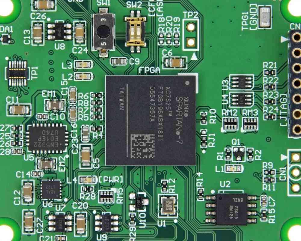
Printed circuit board assembly (PCBA) is the process of soldering electronic components to a PCB or printed circuit board. It is an essential step in manufacturing electronic devices and products. A finished PCBA contains all the necessary electronic components that allow the PCB to perform its intended function.
Some key points about PCBA:
- It follows after PCB fabrication when the bare PCB is manufactured.
- It involves mounting and soldering of components like ICs, resistors, capacitors etc. on the PCB.
- It requires precision and expert skills to ensure quality soldering and avoid errors.
- PCBAs form the core of most electronic gadgets and appliances we use.
- It is an assembly-line manufacturing process in most cases.
- The demand and growth for PCBA services is increasing globally due to rise of complex electronics and need for outsourcing.
So in summary, PCBA is the process of turning a bare PCB into a functional electronic assembly by adding and soldering all the requisite components. It is a crucial step in taking an electronic product design to mass production and market. The quality and efficiency of PCBA has direct impact on the product functioning, reliability and life cycle.
Stages in PCBA Manufacturing Process (h2)
The typical PCBA production process involves the following key stages:
1. Component Procurement (h3)
The first step is procuring all the required components specified in the bill of materials (BOM). This includes active components like ICs, transistors and passive components like resistors, capacitors, diodes etc. Some key aspects here:
- Ensure all components meet the engineering spec needs and quality standards.
- Supplier validation and audit helps mitigate receiving defective or counterfeit parts.
- Managing inventory well by ordering optimal quantities.
2. Solder Paste Printing (h3)
This step prepares the PCB pads for component mounting by applying solder paste on them. Solder paste contains solder metal alloy particles suspended in flux. Some points:
- Solder paste is applied on PCB pads via stencil printing.
- The stencil has cutouts matching the PCB footprint to allow applying paste only on required pads.
- Proper solder paste printing ensures accurate deposit of paste for robust solder joints.
- Parameters like stencil design, paste type and printer setup impact paste print quality.
3. Component Placement (h3)
Electronic components are now placed on the PCB pads with solder paste printed on them. This can be done manually or using automated pick-and-place machines.
- Smaller components are often placed manually using tweezers while larger ones use pick-and-place machines.
- Component placement precision is vital for avoiding assembly errors and quality issues like short circuits.
- Factors considered include location, orientation, alignment and posture of placed component.
4. Soldering and Reflow (h3)
After component placement, soldering is done to establish robust electrical and mechanical connections. There are two main techniques:
Wave Soldering
- Used for PCBAs with through-hole components.
- PCB passes over a wave of molten solder to solder the leads.
Reflow Soldering
- Used for surface-mount components.
- The PCB assembly passes through a reflow oven with heating zones.
- The solder paste melts, joins pads and component leads forming solder joints.
- Parameters like temperature and time profile must be optimized for defect-free soldering.
- Common defects are insufficient solder, solder bridges etc. which must be avoided.
5. Cleaning and Inspection (h3)
Post soldering, cleaning and inspection complete the PCBA production process:
- Flux residues are cleaned using solvents to avoid corrosion or insulation issues.
- Automated optical inspection (AOI) checks PCBA for defects like missing components or faulty solder joints.
- Flying probe testing verifies electrical connections on the PCB.
- Assembly defects caught here can be reworked before final testing.
6. Final Testing and Packaging (h3)
The finished PCBA undergoes comprehensive testing and verification before delivery:
- Functional testing against specifications using test fixtures.
- Burn-in testing under environmental stress to weed out early failures
- Programming firmware or bios code if applicable.
- Quality checks to meet regulatory standards.
- Protective packaging for shipment to customer.
Key Factors Impacting PCBA Quality and Efficiency (h2)
The major aspects influencing PCBA quality, yields and productivity include:
Process Capabilities (h3)
- Soldering equipment maintenance and calibration
- Capability to assemble fine-pitch components
- Expertise in process troubleshooting and optimization
- Adopting technology like automated solder paste inspection
Supply Chain Management (h3)
- Vendor evaluation for defect-free components
- Inventory management to avoid stock-outs or wastage
- Proper storage, handling and moisture control
Quality Systems (h3)
- Process control and workmanship standards
- Inspection criteria aligned with end product needs
- Traceability for change control and defect analysis
- Tools like statistical process control (SPC)
Personnel Skills (h3)
- Operator training on soldering techniques and inspection
- IPC certification for processes like soldering and inspection
- Knowledge of repair and rework of PCB assemblies
ERP and Data Analysis (h3)
- Automated data collection and analysis
- Production dashboard for monitoring key performance indicators (KPIs)
- Data analytics for continuous improvement
Key Indicators for Measuring PCBA Process Performance (h2)
| Metric | Description |
|---|---|
| First Pass Yield (FPY) | Percentage of good boards passed in first attempt |
| Production Yield | Number of good PCBAs / Total attempted |
| Defect Rate | Number or ppm of defective boards |
| Process Capability | Cpk/Ppk indexes for process stability |
| Repair Rate | Percentage of boards needing rework |
| Line Utilization | Percentage of scheduled production time used |
| On Time Delivery | Delivery to commitment date |
Factors to Consider in Selecting a PCBA Production Partner (h2)
Choosing the right electronics manufacturing services (EMS) partner for PCBA production requires evaluating various factors:
- Technical capabilities – Skills in SMT, through-hole, mixed assembly. Fine-pitch assembly expertise.
- Quality certifications – ISO 9001, IATF 16949 show quality commitment.
- Vertical integration – Having in-house PCB fabrication, testing, box build.
- Tooling and equipment – Latest component placement machines, soldering tech.
- Geographic proximity – Physical closeness allows better partnership.
- Scalability – Ability to support fluctuating production volumes.
- Supply chain management – Inventory, logistics, vendor base depth.
- Value-added services – Design support, test development, repair help.
- Cost structure – Pricing model (turnkey vs consignment). Economies of scale.
- Proven track record – Experience with similar electronics products. Known brand name.
Selecting an ideal PCBA partner requires in-depth due diligence on the above parameters to meet product quality goals, cost targets and time-to-market needs.
Trends Shaping the Future of Electronics Assembly (h2)
Some key trends that will influence PCBA manufacturing in the years ahead:
- Miniaturization – Continued demand for assembling smaller, high-density PCBs.
- Heterogeneous integration – Combining different process technologies on a PCB.
- Additive manufacturing – 3D printing of PCB substrates and embedded passives.
- Automation – Wider use of smart storage, automated inspection etc.
- IoT and data analytics – Connected factory with real-time data collection.
- Sustainability – Focus on waste reduction, energy savings, greener chemistries.
- Supply chain resilience – Dual sourcing, nearshoring, buffer inventory.
PCBA for Prototyping vs Mass Production (h2)
PCBA process differs based on whether it is for prototyping or volume production:
| Parameter | Prototyping | Mass Production |
|---|---|---|
| Assembly Type | Low volume, manual assembly | High volume automated assembly |
| Components | Often use readily available parts | Parts approved based on engineering BOM |
| Soldering Method | Manual soldering | Automated SMT assembly and/or wave soldering |
| Inspection | Functional testing and visual inspection | Automated optical inspection, ICT, functional test |
| Lead Time | Typically few days to 2 weeks | Depends on production volumes |
| Cost | Higher cost per board | Lower cost due to economies of scale |
| Flexibility | Design changes possible | Limited flexibility once process is optimized |
| Application | Concept proving, design verification, early testing | Ramping to mass production volumes |
FQA (h2)
What are the main advantages of automated SMT assembly vs manual soldering? (h3)
Some benefits of automated SMT component assembly and soldering are:
- Higher throughput and consistency compared to manual work.
- Greater precision and accuracy in component placement.
- Ability to handle very fine-pitch components not possible manually.
- Eliminates human errors and variations in workmanship.
- Allows traceability from component placement to solder joint quality.
- Frees up skilled staff for more value-added manual tasks.
- Overall improvement in productivity and quality.
What key steps are needed to prepare a PCB design for assembly? (h3)
Some key design for assembly (DFA) steps are:
- Standardize on approved manufacturer component libraries.
- Define solder mask and silkscreen for all layers.
- Add testpoints, fiducials and assembly tooling holes as needed.
- Specify pad shapes, sizes and clearance for easy soldering.
- Minimize board density for manufacturability if possible.
- Review design with assembler feedback before finalizing.
How are BGAs and otherhidden solder joints inspected post PCBA? (h3)
For inspecting hidden solder joints like BGAs:
- 2D X-ray imaging is commonly used to view underneath the component.
- It can detect issues like shorts, opens, voids, insufficient solder.
- Automated optical inspection can also check pad fillet profiles around perimeter of BGAs.
- For process validation, some hidden joints may need to be cross-sectioned and inspected under microscope.
What are some quick tips to improve PCBA first pass yield? (h3)
Some tips to improve PCBA first pass yield:
- Ensure high quality PCBs – avoid etch issues causing shorts.
- Validate and monitor performance of solder paste printer.
- Use optimized SMT program with accurate placement data.
- Validate reflow profile and oven maintenance.
- Implement solder paste inspection.
- Audit defect sources with pareto charts.
- Strengthen process control and operator training.
How can ESD damage be prevented during PCB assembly? (h3)
Some ways to prevent ESD damage during PCBA:
- Use ESD safe packaging for PCBs and components.
- All assembly staff should wear ESD wrist straps grounded to same point.
- Use ESD mats on work benches and ground them.
- Ionizers to neutralize static charges.
- ESD protective storage racks and carriers.
- Label ESD-sensitive boards and components clearly.
- Conduct regular ESD audits and testing.


0 Comments