
Introduction to PWB Assembly
Printed wiring board (PWB) assembly, also known as printed circuit board (PCB) assembly, is the process of soldering and assembling electronic components onto a PWB. A PWB provides the electrical connections between components using copper traces etched from copper sheets laminated onto a non-conductive substrate. PWB assembly is an essential step in manufacturing electronic devices and components.
The PWB assembly process involves several key steps:
- PWB design and fabrication
- Component placement
- Solder paste application
- Component insertion
- Reflow soldering
- Inspection and testing
Proper PWB assembly requires attention to detail, the right tools and processes, and quality standards to ensure the reliability of the end product. This guide provides a comprehensive overview of PWB assembly, including the steps, equipment, processes, and standards involved.
PWB Design and Fabrication
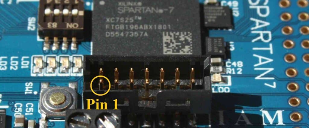
Before assembly can begin, the PWB itself must be designed and fabricated. PWB design is generally done with CAD software that allows for schematic capture and PCB layout. Some key considerations in PWB design include:
- Component placement – efficient and logical placement of components for manufacturing and performance
- Routing – creating copper traces to connect components
- Layer stackup – selecting the number of conductive and dielectric layers
- Materials – FR-4 glass epoxy is common but others exist for high frequency or flexibility
- Hole sizes – for through-hole component leads
- Finishes – typically HASL (hot air solder leveling) or immersion silver
- Solder mask – epoxy layer over copper traces for insulation
- Silkscreen – printable layer for markings like component designators
Once designed, the PWB fabrication process typically involves:
- Imaging – using photoresists and UV light to transfer the trace pattern onto copper laminate
- Etching – chemically removing unwanted copper to leave the desired traces
- Hole drilling – mechanically drilling holes for vias and component leads
- Plating – electroplating conductive layers into drilled holes and edges
- Lamination – bonding etched copper layers together using dielectric/epoxy prepreg
- Solder mask application – coating with epoxy solder mask and etching to reveal pads
- Silkscreen printing – applying epoxy ink layer for markings
- Scoring – cutting individual PWB panels from the fabrication panel
- Electrical testing – validating conductivity and checking for defects
High quality PWB fabrication is critical for reliable PWB assembly and performance of the end product.
PWB Fabrication Methods
There are a few different methods used for fabricating PWBs:
- Subtractive – Starts with a copper clad laminate that is selectively etched away to leave the desired copper trace pattern. Most common method.
- Additive – Starts with a bare substrate and selectively electroplates the copper traces onto the surface. Used for more complex boards.
- Semi-additive – Combines subtractive etching and additive plating. Provides fine trace capability.
- High density interconnect (HDI) – Uses blind and buried vias to build up layers, allowing for denser component mounting. Used in advanced PWBs.
- Any-layer HDI – Further evolution of HDI with an increased number of high density layers possible. Enables complex flex-rigid designs.
Solder Paste Application
Before component placement can begin, solder paste is applied to the pads and lands on the PWB surface. Solder paste consists of tiny solder balls mixed with flux and binder/stabilizing compounds. It comes in jars or cartridges for dispensing. Proper solder paste application helps ensure reliable solder joints post reflow.
Some key parameters in solder paste application:
- Printing – solder paste can be applied by screen printing, stenciling or jetting
- Height – thickness of solder paste after print, typically 100-150 microns
- Tackiness – stickiness of paste to hold components
- Slump – resistance to slumping or spreading after print
- Solder ball size – particle size distribution, typically 25-45 microns
- Alloy – composition like SAC305 or Sn/Pb
- Flux type – no clean or rosin options
Machines like automatic screen printers handle rapid and precise solder paste application onto PWBs. Proper storage, preparation, and inspection of solder paste is also key.
Component Placement
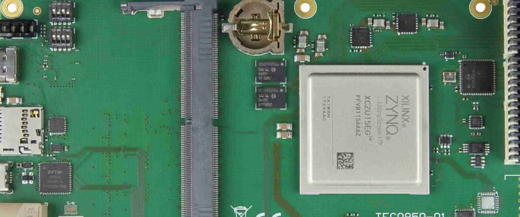
Once solder paste has been applied, the next step is populating the PWB with the required electronic components. This includes passive components like resistors, capacitors, and inductors as well as active components like integrated circuits (ICs) and connectors.
Component placement involves picking components from feeders and placing them onto the PWB with high positional accuracy. This is typically done with automated pick and place machines that use vision systems and feeders loaded with components. Some key considerations for component placement include:
- Component packaging – suitable for automated pickup such as tape and reel
- Pickup heads/nozzles – proper nozzles to handle each component
- Feeder setup – organized component reels for efficient pickup
- Placement speed – parts per hour placement capability
- Placement accuracy – typically 0.1mm or better for fine pitch parts
- Programming – optimizing placement sequences and feeder setup
After placement, glue dots are often used to temporarily hold high standoff components in place. The board then moves to the soldering phase.
Reflow Soldering
Once all components are populated onto the PWB, the assembly passes through a reflow oven to permanently solder the components. The solder paste deposits are melted to create solder joints between pads and component leads. There are a few reflow methods:
Vapor phase reflow uses vapor condensation to uniformly heat the assembly and reflow the solder. More gentle heating can help with large boards or high component mass.
Convection reflow blows hot forced air across the assembly. Different zones heat up and cool down the assembly. Fans provide rapid heating and cooling.
Infrared reflow uses IR lamps and emitters to directly heat the assembly. Provides fast heating rates ideal for small boards. Susceptible to shadowing.
Wave soldering pumps molten solder in a wave to solder bottom side components in a dual pass process with reflow. Used for through-hole components.
The reflow profile must have the right temperatures, ramps, and times to ensure solder joint integrity. Solder paste flux acts to remove oxides while molten but must be properly activated with the right thermal profile.
After soldering, visual inspection and testing helps verify proper solder connections have been made.
Other Assembly Processes
In addition to soldering, PWB assembly may require other manufacturing processes:
- Conformal coating – applying protective epoxy, acrylic, or urethane coatings over the PWB for insulation, chemical resistance, and moisture protection. Typically deposited by spraying or selective coating.
- Potting – Filling enclosures with epoxy resin to protect and strengthen solder joints from vibration, shock, and contamination. Done for ruggedized assemblies. Dispensing and cure oven used.
- Press-fit interconnects – Press-fitting components with compliant pins into plated thru holes to create gas tight interconnections without soldering. Often used for connectors or in high temperature boards.
- Staking – Bonding components to the PWB surface with epoxy for mechanical strength. Requires selective application and cure oven.
- Conformal shielding – Depositing conductive coatings over circuits for EMI shielding. Done using spray, plating, conductive paints/epoxies.
- Rework -Removing and replacing defective components found during testing. Done manually or with special rework machines.
Inspection and Testing
Thorough inspection and testing ensures the quality and reliability of the PWB assembly. Some common quality tests include:
- Visual inspection – looking for defects like missing or misaligned components, poor solder joints, scratches, or foreign objects. AOI machines automate optical inspection.
- X-ray inspection– detects defects hidden from visual inspection like shorts, opens, voids in solder joints. Requires x-ray imaging equipment.
- Flying probe testing – electrically probes test points to verify connectivity and analog performance of the assembly.
- Boundary scan testing – uses boundary scan cells in chips to isolate and test sub-sections of digital logic. Requires programming.
- Functional testing – exercising the board with electrical inputs/loads to verify proper functionality at the system level. Done through fixture or in-circuit testing.
Statistical process control tracking and capability analysis ensures processes are stable, capable, and driving towards zero defects. Failed boards undergo troubleshooting, repair, and root cause analysis.
PWB Assembly Standards
Several standards help define processes, acceptability requirements, and best practices for PWB assembly:
- IPC-A-610 – Acceptability standard for electronics assemblies from IPC, covering criteria for quality solder joints and other defects. Widely used for inspection.
- IPC J-STD-001 – Soldering assembly standard from IPC, including materials, methods, cleanliness, and acceptance criteria. Governs PWB assembly workmanship.
- IPC-A-620 – Acceptability standard for cable, wire, and harness assemblies. Applies to cables mounted on boards.
- IPC-7711/7721 – Rework, modification, and repair of electronics assemblies. Used for rework limits and repair criteria.
- IPC-6012 – Rigid PWB qualification and performance standard. Defines test specs like thermal stress, vibration, and life testing.
- IPC-6013 – Flexible circuit qualification standard. Performance criteria tailored to flex circuits.
Adhering to these standards ensures quality, reliability, and consistency across the electronics industry. They represent decades of expertise and best practices by industry leaders. Certification programs are also available to validate qualifications and capabilities.
PWB Assembly Equipment
PWB assembly requires a variety of specialized equipment to place, solder, inspect, and test boards. Here are some of the key types of equipment:
- Solder paste printer – Prints solder paste using stencils or screens. Handles solder application.
- Pick and place machine – Automates high speed component placement onto boards. Some support very fine pitch.
- Reflow oven – Provides thermal profiling to reflow/melt solder paste and attach components. Convection, vapor phase, infrared ovens used.
- Wave solder machine – Creates wave of molten solder to solder bottom side components in a dual-pass process along with reflow.
- Selective soldering – Targeted soldering of specific joints via mini-wave, dedicated irons, or jetting systems. Lower throughput than wave.
- Inspection machine – Automates optical inspection of solder joints, parts, markings. 3D AOI systems provide magnification and imaging.
- Flying probe tester – Electrically probes nets and nodes to verify connectivity and analog performance of populated boards.
- Boundary scan tester – Tests digital logic sections by programming and reading boundary scan cells embedded in ICs.
- Fixtures – Custom test fixtures used for powering up boards and performing in-circuit tests of functionality.
- Rework machine – Specialized systems to selectively heat and remove components for rework and repair. Some support advanced package types.
The appropriate equipment helps maximize quality, throughput, and reliability when assembling PWBs in volume production.
Summary of the PWB Assembly Process
In summary, here are the key steps in assembling a printed wiring board:
- PWB fabrication using processes like photolithography and lamination to produce the bare board.
- Solder paste application using stencil printing to deposit solder paste onto pads.
- Component placement with pick and place machines to accurately populate components.
- Reflow soldering in ovens to melt solder and attach components.
- Additional assembly processes like conformal coating or potting as required.
- Inspection using automated optical, x-ray, electrical testing to verify quality.
- Rework or repair of any defective assemblies.
Proper process controls, standards adherence, and quality management ensures that PWB assembly produces a reliable, functioning board ready for integration into an electronic product. While the process involves many steps, following best practices and using the right equipment allows efficient and high-yield assembly at scale.
Frequently Asked Questions
What is the difference between PCB and PWB?
PWB stands for printed wiring board while PCB stands for printed circuit board. They are generally synonymous terms referring to the board substrate that connects electronic components using traces. PWB emphasizes the wiring interconnect aspect while PCB emphasizes the printed circuit aspect.
How are very small 0201 or 01005 components handled in assembly?
With 0201 and 01005 sized components becoming more common, specialized pick-and-place machines and processes may be required. Feeders with tape and cover tape designed for these small packages are used along with pick-up heads that can handle the size. High accuracy placement coupled with solder paste printing technology like laser-cut stencils allow reliable assembly.
What is HAL or lead-free soldering?
HAL stands for hot air leveling and refers to the final PWB surface finish. Lead-free solders like SAC alloys have replaced traditional tin-lead solders to eliminate hazardous lead. Lead-free reflow requires higher peak temperatures and proper profiling but can produce reliable solder joints.
How are integrated circuits assembled prior to PWB mounting?
ICs themselves are assembled and packaged first before being mounted on a PWB. The bare IC die is assembled into a package substrate, wire bonded, and then encapsulated in a protective plastic case in a process called transfer molding prior to PWB mounting.
What is the head-in-pillow defect?
A head-in-pillow defect occurs when the solder joint fillet does not properly wet up the sides of the component lead. It leaves the component sitting up on a pillow of solder rather than properly wetting around the lead. It can lead to weakened solder joint reliability.