In the world of printed circuit board (PCB) design and manufacturing, quality assurance is of paramount importance. Ensuring the reliability and proper functioning of PCBs is crucial for the success of electronic products and systems. To achieve this, various testing methods are employed throughout the PCB development and production lifecycle. This article explores seven essential PCB testing methods, including in-circuit testing, highlighting their purposes, techniques, and significance in maintaining high-quality standards.
1. In-Circuit Testing (ICT)
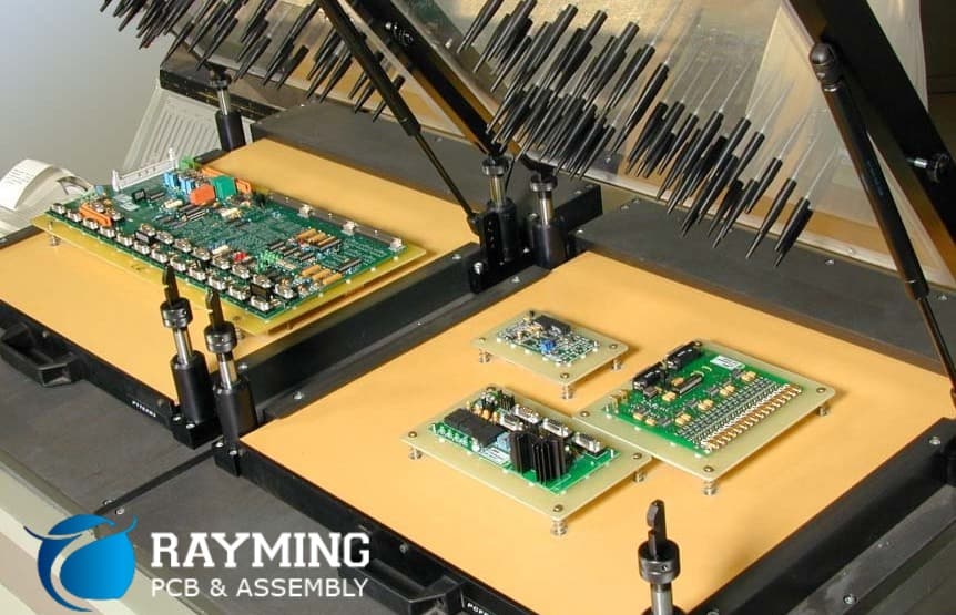
In-circuit testing (ICT) is a widely used testing method for PCBs that involves examining the functionality and connectivity of individual components on the board while they are still in their assembled state. This test is typically performed after the PCB assembly process, but before the final system integration.
How In-Circuit Testing Works
ICT utilizes a specialized test fixture, often referred to as a “bed-of-nails,” which comprises numerous spring-loaded probes or pins that make electrical contact with specific test points on the PCB. These test points are strategically placed on the board during the design phase to allow access to various components and their associated circuitry.
The ICT system applies a series of test signals and voltage levels to the components through the probes, while simultaneously measuring the responses or outputs. These measurements are then compared against predefined reference values or expected results to determine if the components are functioning correctly and if the interconnections between them are intact.
ICT is particularly effective in detecting various types of faults, such as:
- Open circuits (broken connections)
- Short circuits (unintended connections)
- Incorrect or misplaced components
- Defective or out-of-specification components
- Solder defects (shorts, opens, or cold solder joints)
By identifying these faults early in the production process, ICT helps minimize the costs associated with rework and repair, as well as preventing potential failures in the field.
2. Automated Optical Inspection (AOI)
Automated optical inspection (AOI) is a non-contact, vision-based testing method that utilizes high-resolution cameras and advanced image processing algorithms to inspect PCBs for physical defects and manufacturing anomalies.
How Automated Optical Inspection Works
AOI systems capture detailed images of the PCB from multiple angles, often using different lighting conditions and magnification levels. These images are then analyzed by sophisticated software algorithms that compare the captured data against predefined reference images or CAD data for the specific PCB design.
The AOI software can detect a wide range of defects, including:
- Missing or misaligned components
- Incorrect component polarity or orientation
- Solder defects (shorts, opens, bridges, or insufficient solder)
- Contamination or debris on the PCB surface
- Scratches, dents, or other physical damage
AOI is typically performed at various stages of the PCB manufacturing process, such as after solder paste application, component placement, and final assembly. By identifying defects early, AOI helps minimize rework costs and improves overall product quality.
3. Functional Circuit Testing (FCT)
Functional circuit testing (FCT), also known as functional testing or system testing, is a comprehensive testing method that evaluates the overall functionality and performance of a PCB or electronic assembly within its intended operating environment.
How Functional Circuit Testing Works
FCT involves applying a series of input signals or test vectors to the PCB or system and monitoring the corresponding outputs or responses. These inputs and outputs can be digital, analog, or a combination of both, depending on the nature of the circuit or system under test.
During FCT, various parameters and characteristics are measured and analyzed, including:
- Signal integrity and timing
- Power consumption and efficiency
- Electromagnetic interference (EMI) and susceptibility
- Thermal performance and heat dissipation
- Compliance with industry standards and specifications
FCT is typically performed after the PCB assembly process and may involve the use of specialized test equipment, such as signal generators, power supplies, oscilloscopes, and logic analyzers. It is an essential step in validating the overall functionality and performance of the PCB or system before it is released for production or deployment.
4. Boundary Scan Testing
Boundary scan testing is a highly effective testing method for PCBs that utilizes the IEEE 1149.1 standard, also known as the Joint Test Action Group (JTAG) standard. This testing technique is particularly useful for complex, high-density PCBs and systems with limited physical access to test points.
How Boundary Scan Testing Works
Boundary scan testing relies on specialized test circuitry, referred to as boundary scan cells, which are integrated into the design of the PCB’s components, such as integrated circuits (ICs) and programmable logic devices (PLDs). These boundary scan cells are connected in a serial chain, forming a dedicated test path around the boundaries of the device.
During boundary scan testing, a dedicated test controller communicates with the boundary scan cells through the JTAG interface, enabling the following testing capabilities:
- Testing of interconnections between devices
- Testing of individual device functionality
- Testing of programmable logic devices
- Monitoring and controlling device I/O pins
Boundary scan testing offers several advantages, including improved test coverage, reduced physical access requirements, and the ability to test complex boards and systems with limited test points. It is particularly beneficial for highly integrated and dense PCB designs, where traditional testing methods may be ineffective or impractical.
5. Flying Probe Testing
Flying probe testing is a highly flexible and efficient testing method that utilizes a movable test probe or set of probes to make electrical contact with various test points on a PCB.
How Flying Probe Testing Works
In flying probe testing, a PCB is placed on a testing surface, and a specialized test probe or probe head moves across the board, making contact with specific test points as defined by the test program. The probe head can be equipped with various measurement capabilities, such as resistance, capacitance, and continuity testing.
The flying probe testing system is controlled by software that coordinates the movement of the probe head and the application of test signals or measurements. This allows for a high degree of flexibility, as the test program can be easily modified or updated to accommodate different PCB designs or test requirements.
Flying probe testing is particularly useful for prototyping and low-volume production, as well as for testing PCBs with complex geometries or densely populated components. It eliminates the need for dedicated test fixtures, reducing setup costs and enabling rapid testing iterations.
6. X-Ray Inspection
X-ray inspection is a non-destructive testing method that utilizes high-energy electromagnetic radiation to examine the internal structure and integrity of PCBs and electronic assemblies.
How X-Ray Inspection Works
During x-ray inspection, the PCB or assembly is placed between an x-ray source and a detector. As the x-rays pass through the PCB, they are attenuated or absorbed by the various materials and components, creating a detailed image or radiograph on the detector.
X-ray inspection systems often employ advanced imaging techniques, such as computed tomography (CT) or laminography, which provide three-dimensional (3D) representations of the PCB’s internal structure. These 3D images can be analyzed to detect defects and anomalies that may not be visible from the surface, such as:
- Voids or porosity in solder joints
- Cracks or delamination in the PCB substrate
- Misalignment or tilt of components
- Presence of foreign objects or contaminants
X-ray inspection is widely used in the electronics industry for quality control, failure analysis, and process optimization. It is particularly valuable for high-reliability applications, such as aerospace, defense, and medical devices, where the integrity of internal connections and structures is critical.
7. Environmental Stress Screening
Environmental stress screening (ESS) is a testing method that subjects PCBs or electronic assemblies to various environmental stresses, such as temperature cycling, vibration, and power cycling, to identify potential weaknesses or defects that may lead to premature failures.
How Environmental Stress Screening Works
During ESS, PCBs or assemblies are exposed to a series of controlled environmental stresses that simulate the conditions they may encounter during their operational lifetime. These stresses can include:
- Temperature cycling (hot and cold extremes)
- Vibration or shock testing
- Power cycling (power-on and power-off cycles)
- Humidity exposure
- Thermal shock (rapid temperature changes)
The purpose of ESS is to accelerate the process of identifying and removing weak or defective components, interconnections, or assemblies that may fail prematurely under normal operating conditions. By subjecting PCBs or assemblies to these extreme environmental stresses, any latent defects or potential weaknesses are likely to manifest themselves, allowing for early detection and correction.
ESS is often used in conjunction with other testing methods, such as functional testing or in-circuit testing, to ensure the reliability and robustness of PCBs and electronic assemblies, particularly in critical applications where failure is not an option.
Table: Summary of PCB Testing Methods
| Testing Method | Purpose | Key Advantages |
|---|---|---|
| In-Circuit Testing (ICT) | Verifies functionality and connectivity of individual components | Early detection of faults, cost-effective |
| Automated Optical Inspection (AOI) | Detects physical defects and manufacturing anomalies | Non-contact, high inspection speed |
| Functional Circuit Testing (FCT) | Evaluates overall functionality and performance | Comprehensive system-level testing |
| Boundary Scan Testing | Tests interconnections and device functionality | Improved test coverage, limited physical access required |
| Flying Probe Testing | Flexible electrical testing without dedicated fixtures | Cost-effective for prototyping and low-volume production |
| X-Ray Inspection | Examines internal structure and integrity | Non-destructive, detects internal defects |
| Environmental Stress Screening (ESS) | Identifies potential weaknesses under environmental stresses | Accelerates defect detection, improves reliability |
Frequently Asked Questions (FAQ)
- Why is PCB testing important? PCB testing is crucial for ensuring the reliability, functionality, and quality of electronic products and systems. It helps identify defects, faults, and potential weaknesses early in the manufacturing process, minimizing the risk of field failures, reducing costs associated with rework and repair, and maintaining high-quality standards.
- When should different PCB testing methods be applied? The choice of PCB testing method depends on the stage of the product lifecycle and the specific objectives of the testing. For example, in-circuit testing and automated optical inspection are typically performed during the assembly process, functional circuit testing is conducted after assembly, and environmental stress screening is often used as a final step before product release.
- Can multiple PCB testing methods be combined? Yes, it is common practice to combine multiple PCB testing methods to achieve comprehensive coverage and ensure the highest level of quality and reliability. For instance, in-circuit testing may be followed by functional circuit testing and environmental stress screening to thoroughly evaluate the PCB or assembly.
- What are the advantages of automated testing methods like AOI and boundary scan testing? Automated testing methods, such as automated optical inspection (AOI) and boundary scan testing, offer several advantages over manual testing techniques. These include increased inspection speed, improved consistency and repeatability, reduced human error, and the ability to test complex and high-density PCBs more effectively.
- How do environmental stress screening and x-ray inspection contribute to product reliability? Environmental stress screening (ESS) helps identify potential weaknesses or defects that may lead to premature failures by subjecting PCBs or assemblies to extreme environmental conditions. X-ray inspection, on the other hand, allows for the non-destructive examination of internal structures and interconnections, enabling the detection of defects that may not be visible from the surface, contributing to improved reliability and quality assurance.


0 Comments