Electronic Components Assembly: A Guide to Manufacturing PCBAs
Introduction to Electronic Components Assembly
The assembly of electronic components onto printed circuit boards (PCBs) is a critical step in the electronics manufacturing process. This assembly, commonly referred to as PCBA (Printed Circuit Board Assembly), involves soldering various electronic components like resistors, capacitors, integrated circuits (ICs), transistors etc. onto a PCB. The completed board with all components soldered is called an assembled PCB.
PCBA is done manually or using automated processes. Manual assembly is labor-intensive and is usually employed for low volume production runs. Automated assembly uses specialized equipment for high volume manufacturing.
The steps involved in assembling electronic components on PCBs are:
PCB Fabrication
The bare PCB is fabricated first with copper tracks connecting component pads.
Stencil Printing
Solder paste is applied on PCB pads where components will be placed, using stencils.
Component Placement
Components are accurately placed on corresponding pads on the PCB.
Soldering
The board passes through a reflow oven melting the solder paste to form solder joints to attach components.
Cleaning
Excess flux is removed from the soldered board.
Testing and Inspection
The fully assembled board is tested for defects.
Key Components for PCB Assembly
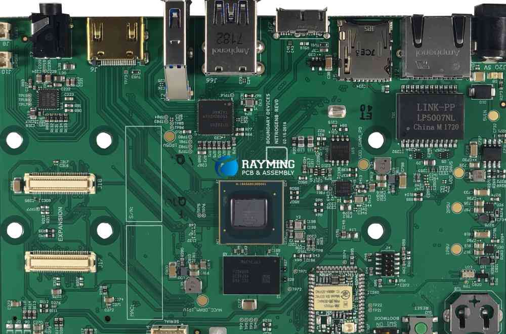
Some of the major electronic components assembled on PCBs are:
Resistors
Resistors restrict current flow. Common types are carbon film, metal film, wire wound, etc.
Capacitors
Capacitors store electric charge. Various types like ceramic, electrolytic, and tantalum capacitors are used.
Diodes
Diodes allow current to flow in only one direction. Light Emitting Diodes (LEDs) emit light when current flows through them.
Transistors
Transistors amplify or switch electric signals and power. They are used extensively in electronic circuits.
Integrated Circuits (ICs)
ICs contain microcircuits with hundreds of components like diodes, transistors, resistors fabricated on a silicon chip. ICs perform varied functions.
Inductors
Inductors store energy in their magnetic fields. They are coils of wire used in filters and power supplies.
Switches
Switches interrupt current flow. Toggle switches, push button switches, DIP switches are used on PCBs.
Connectors
Connectors like headers, edge connectors, and USB ports provide connection points on the board.
Light Emitting Diodes (LEDs)
LEDs provide visual indicators on electronic devices. Infrared LEDs are used for remote controls.
PCB Assembly Techniques
There are several techniques used for assembling electronic components onto PCBs:
Through-Hole Assembly
In through-hole assembly, component leads are inserted through holes in the PCB and soldered to pads on the other side. Boards with through-hole components are also referred to as Through Hole Technology (THT) boards.
Surface Mount Assembly
Surface mount components have terminations that allow mounting directly onto pads on the PCB surface. This process is known as Surface Mount Technology (SMT).
Mixed Technology Assembly
Many modern PCBAs use both through-hole and SMT components. This is known as mixed technology assembly.
Sequential vs Simultaneous Assembly
With sequential assembly, through-hole components are soldered first. SMT components are then assembled in following steps. In simultaneous methodology, both through-hole and SMT components are placed and soldered in one reflow step.
PCB Assembly Process Steps
The major steps in assembling components on a PCB are:
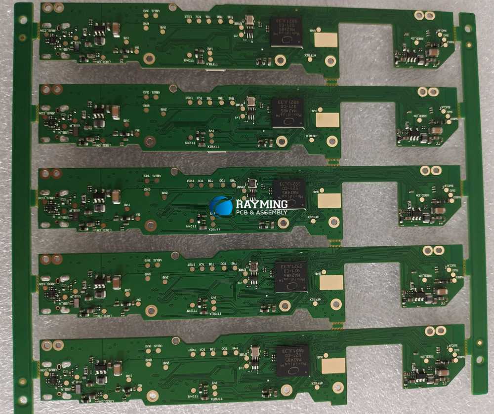
1. PCB Fabrication
The bare PCB is fabricated with copper tracks connecting component pads where parts will be assembled. The board surface is coated with solder mask and silkscreen.
A fabricated PCB without components
2. Stencil Printing
Solder paste is applied on PCB pads using metal stencils with cutouts matching the pads. This helps deposit the paste only on required pads.
Stencil printing solder paste on a PCB
3. Component Placement
Components are placed on the solder paste deposits using automated pick and place machines or manually. Machines allow faster and more accurate placement.
Electronic components placed on a PCB
4. Soldering
The PCB then passes through a reflow oven to melt the solder paste. The components are soldered to the board pads forming electrical and mechanical connections.
Soldering components by passing the PCB through a reflow oven
5. Cleaning
Any flux residue remaining after soldering is cleaned off the board using solvents. This prevents corrosion.
6. Testing and Inspection
The fully assembled and soldered PCB is then tested for manufacturing defects and functionality. Automated Optical Inspection (AOI) checks for missing or misaligned components. Boundary scan tests verify interconnects between components using test points incorporated in the PCB design. Flying probe testers perform electrical testing.
7. Conformal Coating
For boards used in harsh environments, a conformal coating of epoxy or acrylic resins is applied. This protects against moisture, dust and corrosion.
Factors Impacting Quality and Reliability
To ensure high quality and reliable PCB assemblies, the following factors need to be controlled:
- Components – Using parts qualified to relevant quality standards
- Solder paste – Using the right alloy with optimal particle size
- Soldering temperature – Avoiding overheating and temperature gradients
- Board handling – Minimizing board flexing and bending
- Cleaning process – Preventing chemical damage and moisture
- ESD control – Grounding personnel, machines, and using ESD safe packaging
- Inspection – Detecting errors early using automated optical, x-ray and flying probe inspection
- Workmanship standards – Setting clear acceptability criteria for solder joints, adhesion etc.
- Documentation – Maintaining detailed build instructions, test procedures and assembly drawings.
Poor process control can lead to defects like open solder joints, bridges between pads, lifted leads, component damage etc. This results in field failures and reduced product reliability.
Advantages of Outsourcing PCB Assembly
Many OEMs outsource PCB assembly to specialized manufacturing services providers. The benefits include:
- Cost Savings: Contract manufacturers have lower operational costs achieved through economies of scale and specialization.
- Focus on Core Competencies: Frees up OEM resources to concentrate on design and marketing activities.
- Quality: Access to advanced assembly equipment and highly trained operators ensures reliable boards.
- Scalability: Quick ramp up and ramp down of production volumes is possible.
- Reduced Time-to-Market: Faster assembly turnaround times compared to in-house.
- Supply Chain Simplicity: Single point of contact for the entire electronics manufacturing and test process.
Finding the Right Assembly Partner
Here are some tips on selecting an EMS provider for PCB assembly:
- Check capabilities – range of assembly technologies (SMT, thru-hole, mixed), in-house vs. outsourced processes, component sourcing abilities.
- Ensure demanding technical requirements can be met – fine pitch SMT, BGAs, high-density boards etc.
- Evaluate quality systems and certifications – ISO 13485, 9001, IPC standards, counterfeit mitigation procedures.
- Assess engineering support – capabilities for DFM analysis, test development, firmware loading, prototyping.
- Validate capacity – evaluate current workloads and scalability.
- Confirm security procedures for intellectual property protection.
- Review financial stability.
- Tour facilities to directly view infrastructure, process controls and housekeeping.
- Check customer references and reputation.
This due diligence helps mitigate overall project risks when outsourcing PCB assembly.
Conclusion
Assembling electronic components onto PCBs involves carefully controlled processes like solder paste printing, accurate component placement, reflow soldering, cleaning and testing. Utilizing a competent contract manufacturer provides OEMs the combined benefits of quality, cost control and faster time-to-market. Carefully selecting an EMS partner using the criteria outlined above allows OEMs to focus on core product development activities. This ultimately results in well-built electronic products that exceed customer expectations and timelines.
Frequently Asked Questions
Q: What are the typical defects observed in PCB assemblies?
A: Common assembly defects include –
- Open or cold solder joints
- Solder bridges between pads
- Wrong component value or orientation
- Poor lead clinching for through-hole parts
- Cracked solder joints
- Lifted PCB pads and tracks
- Electrically overstressed components
- Mechanical damage like cracks
Q: What is the IPC classification for electronics assembly?
A: The IPC-A-610 standard classifies electronics assembly into 3 classes:
- Class 1 – General purpose products
- Class 2 – Dedicated service products. E.g. Communications infrastructure equipment.
- Class 3 – High performance products. E.g. Medical, aerospace and defense electronics.
Q: What are no clean soldering fluxes?
A: No clean fluxes do not require cleaning after soldering. They have minimal residues that are non-conductive and non-corrosive. They allow faster processing without a cleaning step.
Q: What is the difference between lead-free and leaded soldering?
A: Lead-free soldering uses tin-silver-copper or other non-lead alloys owing to environmental regulations. Leaded solder contains tin-lead alloys that melt at lower temperatures.
Q: What are conformal coatings?
A: Conformal coatings are protective layers applied on assembled PCBs. They shield against moisture, dust and corrosion. Common coatings include acrylic, urethane and silicone resins.


0 Comments