
Top Myths and Facts about PCB Prototyping and Assembly
What is PCB Prototyping?
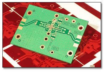
PCB prototyping is the process of creating a prototype printed circuit board (PCB) for testing and validation before mass production. It involves designing the circuit, laying out the components, and fabricating a small number of boards for testing. PCB prototyping is an essential step in the electronics manufacturing process, as it allows designers to test their designs and make any necessary changes before committing to large-scale production.
Benefits of PCB Prototyping
- Identifies design flaws early in the development process
- Allows for testing and validation of the circuit design
- Provides an opportunity to optimize the layout and component placement
- Enables testing of the PCB’s functionality and performance
- Reduces the risk of costly mistakes in mass production
Common Myths about PCB Prototyping
Myth 1: PCB prototyping is expensive
One of the most common misconceptions about PCB prototyping is that it is an expensive process. However, this is not necessarily true. While the initial cost of creating a prototype may be higher than the cost of producing a single board in mass production, it is a worthwhile investment in the long run.
By identifying and addressing design issues early in the development process, PCB prototyping can help avoid costly mistakes and delays in mass production. In fact, the cost of fixing a design flaw after mass production has begun can be significantly higher than the cost of creating a prototype.
Myth 2: PCB prototyping is time-consuming
Another common myth about PCB prototyping is that it is a time-consuming process that can delay the overall development timeline. While it is true that creating a prototype takes time, the benefits of prototyping far outweigh the time invested.
By thoroughly testing and validating the design through prototyping, designers can avoid the need for multiple revisions and redesigns later in the development process. This can ultimately save time and resources in the long run.
Myth 3: PCB prototyping is only necessary for complex designs
Some designers may believe that PCB prototyping is only necessary for complex or high-stakes designs. However, prototyping can be beneficial for projects of all sizes and levels of complexity.
Even simple designs can benefit from prototyping, as it allows designers to test the functionality and performance of the circuit in a real-world setting. This can help identify any issues or areas for improvement before moving forward with production.

Facts about PCB Prototyping
Fact 1: PCB prototyping can be done in-house or outsourced
PCB prototyping can be done either in-house or outsourced to a specialized PCB prototyping service. In-house prototyping requires an investment in equipment and expertise, but it allows for greater control over the process and faster turnaround times.
Outsourcing PCB prototyping to a specialized service can be a cost-effective option, particularly for smaller companies or those without in-house manufacturing capabilities. These services typically offer fast turnaround times and can handle a wide range of design requirements.
Fact 2: PCB prototyping can be done using various methods
There are several methods available for PCB prototyping, each with its own advantages and disadvantages. Some common methods include:
-
3D printing: This method uses a 3D printer to create a physical model of the PCB design. It is relatively quick and inexpensive but may not provide the same level of detail and accuracy as other methods.
-
Milling: This method uses a computer-controlled milling machine to remove copper from a blank PCB substrate, creating the desired circuit pattern. It is a fast and flexible method but may not be suitable for very fine pitch designs.
-
Chemical etching: This method uses a chemical process to remove unwanted copper from the PCB substrate, leaving the desired circuit pattern. It is a high-precision method that can handle very fine pitch designs but requires specialized equipment and expertise.
| Method | Advantages | Disadvantages |
|---|---|---|
| 3D Printing | Quick, inexpensive | Limited detail and accuracy |
| Milling | Fast, flexible | May not handle very fine pitch designs |
| Chemical Etching | High precision, handles fine pitch designs | Requires specialized equipment and expertise |
Fact 3: PCB prototyping can be done at various levels of complexity
PCB prototyping can be done at various levels of complexity, depending on the specific requirements of the project. Some common levels of complexity include:
-
Single-layer PCBs: These are the simplest type of PCB, with all components and traces on a single layer of the board. They are relatively easy to design and manufacture but may not be suitable for more complex circuits.
-
Double-layer PCBs: These PCBs have components and traces on both sides of the board, allowing for more complex circuit designs. They require more advanced manufacturing processes but offer greater flexibility and functionality.
-
Multi-layer PCBs: These PCBs have multiple layers of circuitry separated by insulating layers. They allow for even greater complexity and density but require specialized manufacturing processes and expertise.
| PCB Type | Complexity | Applications |
|---|---|---|
| Single-layer | Low | Simple circuits, low-power applications |
| Double-layer | Medium | More complex circuits, higher power applications |
| Multi-layer | High | Highly complex circuits, high-speed applications |

PCB Assembly
Once the PCB Prototype has been tested and validated, the next step is to move forward with PCB assembly. PCB assembly involves soldering components onto the PCB and preparing it for use in the final product.
Types of PCB Assembly
There are two main types of PCB assembly: through-hole and surface mount.
-
Through-hole assembly: This method involves inserting component leads through holes drilled in the PCB and soldering them in place on the opposite side. It is a reliable and robust method but requires more manual labor and is generally slower than surface mount assembly.
-
Surface mount assembly: This method involves placing components directly onto pads on the surface of the PCB and soldering them in place. It allows for smaller components and higher density designs but requires more precise placement and specialized equipment.
PCB Assembly Process
The PCB assembly process typically involves the following steps:
-
Solder paste application: A thin layer of solder paste is applied to the PCB pads using a stencil or screen printing process.
-
Component placement: Components are placed onto the PCB using automated pick-and-place machines or by hand, depending on the level of complexity and volume.
-
Reflow soldering: The PCB is heated in a reflow oven, melting the solder paste and securing the components in place.
-
Inspection and testing: The assembled PCB is inspected for any defects or errors and tested to ensure proper functionality.

FAQ
How long does PCB prototyping take?
The time required for PCB prototyping depends on various factors, such as the complexity of the design, the prototyping method used, and the workload of the prototyping service. In general, simple designs can be prototyped in a matter of days, while more complex designs may take several weeks.
How much does PCB prototyping cost?
The cost of PCB prototyping depends on factors such as the size and complexity of the design, the number of layers, and the prototyping method used. Simple designs can cost a few hundred dollars, while more complex designs can cost several thousand dollars. It is important to get quotes from multiple prototyping services and to consider the long-term benefits of prototyping in terms of avoiding costly mistakes in mass production.
What are the differences between PCB prototyping and PCB production?
PCB prototyping involves creating a small number of boards for testing and validation, while PCB production involves manufacturing a large number of boards for use in the final product. Prototyping is typically done using different methods and materials than production and may involve more manual labor and specialized equipment. Production is generally more automated and streamlined, with a focus on efficiency and cost-effectiveness.
Can I do PCB prototyping myself?
While it is possible to do PCB prototyping yourself using basic tools and materials, it can be a challenging and time-consuming process. It requires a good understanding of PCB design and manufacturing processes, as well as access to specialized equipment and materials. For most projects, it is generally more efficient and cost-effective to outsource PCB prototyping to a specialized service.
What should I look for in a PCB prototyping service?
When choosing a PCB prototyping service, there are several key factors to consider:
- Experience and expertise in PCB design and manufacturing
- Range of prototyping methods and materials available
- Ability to handle the specific requirements of your project
- Fast turnaround times and competitive pricing
- Good communication and customer support
- Positive reviews and reputation in the industry
It is also a good idea to request quotes and samples from multiple services to compare options and ensure the best fit for your project.
Conclusion
PCB prototyping is a critical step in the electronics manufacturing process that allows designers to test and validate their designs before committing to large-scale production. While there are some common myths and misconceptions about PCB prototyping, the benefits of prototyping far outweigh the costs and time invested.
By understanding the different methods and levels of complexity involved in PCB prototyping, as well as the key considerations for PCB assembly, designers can make informed decisions and optimize their designs for success. Whether done in-house or outsourced to a specialized service, PCB prototyping is an essential tool for bringing innovative electronics products to market efficiently and effectively.