Introduction
Printed circuit boards (PCBs) are essential components in virtually every electronic device we use today. From computers and smartphones to appliances and vehicles, PCBs provide the foundation on which all other components are mounted and interconnected.
There are two main types of PCB construction: through hole and surface mount. This article will focus specifically on through hole PCB assembly. We’ll cover what through hole assembly is, its advantages and disadvantages compared to surface mount, the through hole assembly process step-by-step, and some best practices for designing and assembling through hole PCBs.
What is Through Hole PCB Assembly?
In through hole PCB assembly, components have leads or terminals that are inserted through holes drilled in the PCB and soldered to pads on the opposite side to form both mechanical and electrical connections. The leads and holes are relatively large, typically between 1.0-2.0mm in diameter.
Through hole components with leads inserted through PCB.
Some key advantages of through hole PCB assembly include:
- Simplicity – Through hole assembly is generally easier and more straightforward than surface mount. The larger component leads insert easily through the holes.
- Repairability – It’s relatively easy to desolder and replace individual through hole components. This makes through hole PCBs better suited for prototyping and low volume production.
- Reliability – The through hole mounting process creates very strong mechanical and electrical connections that stand up well to shaking and vibration.
- Compatibility – Most standard electronic components are available in through hole packages, making them easy to source and substitute.
However, through hole assembly also has some disadvantages compared to surface mount technology (SMT):
- Lower component density – Through hole components take up more space on the PCB due to the need for drilled holes and pads. This limits how small and compact a board can be.
- More difficult automation – The manual process of inserting component leads through holes makes through hole assembly much less automated than SMT. This can limit throughput for high volume production.
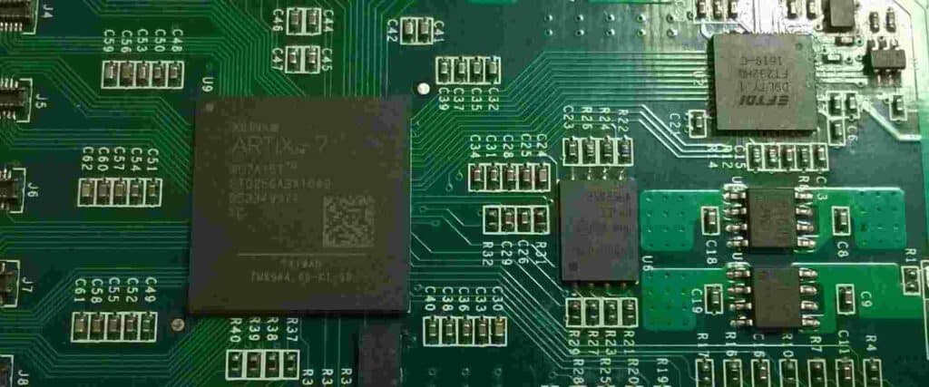
- Not suitable for advanced components – Cutting edge components like CPUs, FPGAs, and some RF/wireless ICs are only available in surface mount packages.
In summary, through hole PCB assembly is best suited for low to medium complexity boards where simplicity, serviceability, and reliability are important, and where overall size and weight are less constrained. Next we’ll look at the step-by-step through hole assembly process.
Through Hole PCB Assembly Process
The typical through hole PCB assembly process consists of the following key steps:
1. PCB Fabrication
The bare PCB is fabricated by a PCB manufacturer. This involves:
- Drilling holes at all component lead insertion points using small (e.g. 0.8mm-1.2mm) mechanical drills.
- Plating the interior hole walls and pads with copper to provide a conductive surface for soldering.
- Covering the entire board surface with solder mask except at the soldering pads.
- Printing a silkscreen layer for markings like component designators.
- Scoring or panelizing multiple boards together for easier handling.
2. Component population
The components are inserted into their corresponding PCB holes either by hand or by automated insertion machines:
- Simple insertion machines range from manual pick-and-place with pneumatic inserters to fully automated vibratory bowl feeders.
- For prototypes and low volumes, manual insertion may be done using tweezers.
3. Soldering
The component leads are soldered to the plated PCB pads to form mechanical and electrical connections:
- Wave soldering involves passing the entire loaded PCB bottom-side down over a waving pool of liquid solder. The solder adheres to the metal surfaces.
- Hand soldering is done individually on each joint, generally only for rework or touch-up.
- Reflow soldering uses solder paste and IR heaters like in SMT assembly but can also be used for through hole components.
4. Cleaning
Any residual flux, solder, or other contaminants are washed off the PCB using cleaners/solvents.
5. Inspection & testing
QC checks help verify proper assembly and catch any defects:
- Visual inspection checks for missing or misaligned components, poor solder joints, damage, etc.
- In-circuit testing verifies electrical connectivity and function between components.
- Functional testing validates the board operates properly as a system.
6. Conformal coating (optional)
A protective plastic coating can be selectively applied to enhance reliability and isolation.
With the assembly process covered, let’s now look at some best practices for through hole PCB design.
Best Practices for Through Hole PCB Design
Here are some key things to keep in mind when designing a PCB for through hole assembly:
- Component spacing – Leave adequate spacing between components and keep sensitive analog circuits separate from high-speed digital or switching circuitry to prevent EM interference.
- Hole diameter – Size holes based on lead diameters. Allow ~1.5x the lead diameter for easy insertion without excessive slop.
- Annular rings – Pads should have sufficient annular rings (clear area around the hole) to prevent solder bridging between pads and traces. 0.6-1mm is typical.
- Via tenting – Cover unused through holes with soldermask (“tenting”) to prevent solder wicking down the hole.
- Soldermask expansion – Expand the soldermask slightly (e.g. 0.1mm) beyond pads to account for misregistration.
- Breakout boards – Use breakout boards or headers to connect off-board components like connectors. This avoids stresses on the solder joints.
- Thermal relief – Use thermal relief cutouts on large copper pads and planes to prevent cracking from differential thermal expansion.
Adhering to these guidelines during the PCB layout process will help avoid many common through hole assembly issues and produce a more reliable, manufacturable board.
Through Hole Assembly Challenges
While through hole assembly is generally straightforward, some potential challenges include:
- Solder bridging – Excess solder can build up and bridge between closely spaced pads. This is remedied by closer component spacing, smaller pad sizes, or lower solder volumes.
- Insufficient solder – If solder volume or pad area is too small, joints may be dry or weakened. Increasing pad and part lead size helps wetting and solder adhesion.
- Excessive component lead bending – Too much lead bending stresses the component and weakens the joint. Appropriately sized holes and carefully controlled insertion depths reduce bending.
- Tombstoning – Misalignment during soldering can result in components standing up on one end like tombstones. This can be prevented with tack adhesive, component lead forming, or reducing temperature gradients.
- Solder voiding – Trapped air and flux gasses escaping can cause voiding inside solder joints leading to reduced strength and conductivity. Proper heating and ventilation during soldering minimizes voids.
With careful process control and inspection, these potential defects can be kept to within acceptable limits for a robust through hole assembly process.
Frequently Asked Questions
Q: What are the main advantages of through hole PCB assembly?
A: The main advantages of through hole assembly are simplicity, repairability, reliability, and compatibility with standard component packages. The large leads and pads are easy to hand solder or insert into automated board assembly machines.
Q: Is through hole technology obsolete compared to SMT?
A: Through hole is not obsolete. It still offers benefits like serviceability and remains widely used for many non-miniaturized electronic products. However, SMT dominates cutting-edge applications like smartphones that require extremely high component density.
Q: How are components held in place prior to soldering?
A: There are a few options to hold components in place before soldering:
- Friction fit of the leads within the plated through holes
- Adhesives like epoxy or tacky flux
- Mechanical clinching/crimping of the component leads
- Small plastic clips or retainers on the bottom side
Q: What are some common SMT components not available in through hole packages?
A: Some components like advanced ICs (e.g. CPUs, FPGAs), QFN packages, fine-pitch BGAs, and 0201/0402 passive components are typically only available in surface mount formats. However, through hole versions of most common component types like resistors, capacitors, transistors, connectors, etc. are readily available.
Q: Can solder joints be repaired on a through hole PCB?
A: Yes, through hole solder joints are repairable. Defective joints can be desoldered with solder wick, flux, and a soldering iron, and components replaced by hand soldering new ones. This is much easier than repairing SMT boards where removing components often damages pads.
Conclusion
Through hole assembly is a proven, reliable PCB fabrication technology suitable for an extremely wide range of electronic products. By following some basic design and assembly best practices, manufacturers can avoid common defects and utilize through hole’s advantages in simplicity, reparability, and compatibility. While advanced miniaturized products will continue transitioning to SMT, through hole maintains a well-deserved place among modern PCB assembly techniques.


0 Comments