
Printed Circuit Board Assembly (PCBA): A Complete Guide
What is Printed Circuit Board Assembly (PCBA)?
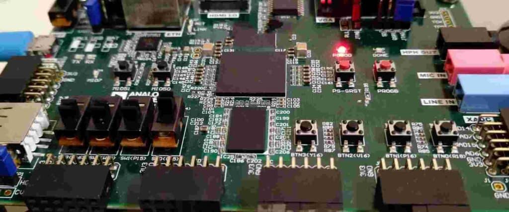
A printed circuit board assembly (PCBA) is a fundamental component of electronic devices that contains a printed circuit board (PCB) populated with electronic components. It provides interconnections between components to form functional circuits that enable the flow of power and signals.
PCBA refers to the process of soldering and assembling various electronic components onto a PCB. The components include passive devices like resistors, capacitors, and inductors, as well as active devices like integrated circuits (ICs), transistors, and diodes. Proper assembly and soldering of these components is critical for the functioning of any electronic product.
Key Steps in PCBA
The PCBA process consists of the following key steps:
- PCB fabrication – The bare PCB is fabricated based on the circuit requirements with traces, pads, vias and layers etched onto the board. Popular materials include FR-4 and polyimide.
- Stencil printing – Solder paste is applied on PCB pads through stencil printing to provide temporary adhesive for component mounting.
- Component placement – Electronic components are precisely placed on the appropriate pads of the PCB. Automated pick-and-place machines are commonly used.
- Soldering – The board passes through a reflow oven or wave soldering system to melt the solder and form permanent solder joints.
- Inspection and testing – Optical inspection and electrical testing validates assembly quality and confirms the board is functioning as designed.
- Conformal coating – A protective coating may be applied to shield the components from environmental factors.
Benefits of PCBA
Some key benefits of PCBA include:
- Efficiency – Automated assembly minimizes production time and costs compared to manual assembly.
- Reliability – Machines ensure uniform solder joint quality for long-term reliability.
- Flexibility – Ability to assemble boards with diverse components, densities and form factors.
- Scalability – Production volumes can be easily scaled to match changing demand.
- Single-source – One supplier provides all services from design, fabrication, assembly and testing.
PCBA Process Flowchart
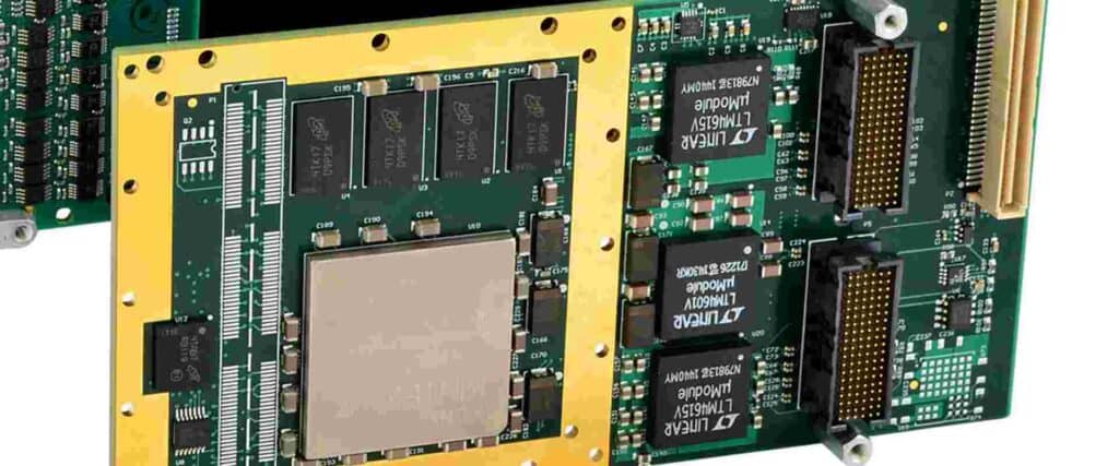
The typical workflow for printed circuit board assembly consists of the following key stages:
As illustrated in the flowchart, the process starts with PCB fabrication based on the electronic circuit design. This is followed by solder paste application, pick-and-place assembly, soldering, cleaning, inspection and testing. Feedback may require iterating some steps to ensure quality standards are achieved.
Surface Mount Technology in PCBA
Surface mount technology (SMT) is the dominant attachment method used for PCBA. In SMT, components are mounted directly onto the surface of the PCB without any leads or holes. The components have metallic pads that align with corresponding pads on the board.
Advantages of SMT
Some major advantages of SMT over through-hole technology are:
- Smaller components enabling miniaturization
- Higher component density with reduced weight
- Faster automated assembly with improved yields
- Cost-effective for high volume production
- Allows double-sided component mounting
- Improved system reliability with shorter leads
SMT Components
Common types of surface mount components used in PCBA include:
| Component | Description |
|---|---|
| Resistors and Capacitors | Available in chip (single component) or array package for multiple devices |
| Inductors | Perfect for RF circuits demanding high Q factor |
| Diodes and Transistors | SOT23, SOT89 and SOT223 are ideal SMT packages |
| Integrated Circuits (ICs) | Chips with multiple gates like microcontrollers, linear ICs, audio ICs etc. |
| Connectors | High density board-to-board, wire-to-board and RF connectors |
| Light Emitting Diodes (LEDs) | Provide illumination and status indicators |
Advanced PCBA Technologies
PCB assembly technologies continue to evolve enabling denser and more reliable electronic products. Some of the advanced technologies include:
Ultra-Fine Pitch Components
Components with pitch under 0.4mm allow dense component packing important for miniaturization. Advanced pick-and-place equipment is required for precision placement.
Chip Scale and Wafer Level Packaging
By eliminating bulky packages and connecting ICs directly to boards, these technologies minimize footprint while enhancing electrical performance.
Embedded Passives
Passive components like resistors and capacitors are fabricated within the PCB layers reducing cost and footprint over discrete devices.
3D Printing of PCBs
Additive manufacturing techniques like stereolithography can 3D print complex multilayer PCBs and encapsulated electronics as a single part.
Flexible and Stretchable Electronics
Boards fabricated on thin flexible and stretchable substrates that integrate advanced materials enable conformal placement over curvilinear surfaces.
Automated Optical Inspection (AOI)
AOI rapidly validates assembly quality for errors in component placement, solder joints, polarity etc. This improves yields and reliability.
JTAG/Boundary Scan Testing
JTAG tools test interconnects between components on assembled boards by applying signals and measuring responses via shift registers on components.
Key Considerations for PCBA
Careful attention must be paid to the following aspects for a successful PCBA process:
- Component selection – Choose components qualified for PCBA processes like soldering temperatures.
- Footprint compatibility – Component footprints must match land patterns on the PCB.
- PCB parameters – Select suitable PCB materials to withstand process conditions.
- Solder paste – Use appropriate solder alloy, sphere size and tackiness.
- Stencil design – Stencil thickness, aperture openings/shapes and alignment aid solder paste transfer.
- Pick-and-place optimization – Consider component size, height, warpage, stacking etc. for optimized placement.
- Reflow profile – Ensure profile has the right ramp-up rate, peak temperature and cooling.
- Inspection points – Strategically inspect assembly quality after critical process steps.
- Protective coatings – Determine if conformal coatings are required for environmental protection.
- DFM/DFA – Design the boards and assembly process for optimized manufacturability.
Careful consideration of these parameters results in high assembly yields and robust electronic products.
FQA
What are the main benefits of PCBA?
Some of the major benefits of printed circuit board assembly include:
- Efficiency through optimized automation and production times
- Improved reliability and repeatability over manual assembly
- Flexibility to assemble diverse components and board types
- Scalability to match production volumes to demand
- Consolidated manufacturing with a single supplier for PCB fabrication through assembly
What is the difference between through-hole and surface mount technology?
The main differences are:
- Through-hole – Leaded components are inserted into holes in the PCB and soldered on the opposite side.
- Surface mount – Components are mounted directly onto the surface of the PCB without leads.
Through-hole allows simple single-sided assembly but takes up more space. SMT enables miniaturization and double-sided mounting but requires advanced pick-and-place equipment.
Why is solder paste printing done in PCBA?
Solder paste printing deposits the right amount of solder paste onto pads on the PCB. This paste temporarily holds the components in place before soldering. Key benefits of solder paste printing are:
- Temporary adhesive to fix components onto board before soldering
- Correct amount ensures optimum solder joint after reflow
- Enables high speed automated assembly
- Solder balls accommodate component misalignment during placement
- Allows inspection of paste deposits before component placement
What is Automated Optical Inspection (AOI) in PCBA?
AOI is imaging-based automated inspection of assembled PCBs using advanced cameras and image processors. It validates assembly quality and catches errors like:
- Missing, misaligned or incorrect components
- Insufficient solder paste deposits
- Bridging between pads
- Faulty solder joints
- Wrong polarity
AOI improves quality control, minimizes defects and prevents costly rework.
Why is DFA important for PCBA?
Design for Assembly (DFA) optimizes the PCB design and component selection for ease of assembly. Important DFA guidelines are:
- Standardized component packages and footprints
- Minimum component height variations
- Adequate spacing between components
- Simple and symmetrical placement
- Double-sided component placement where possible
- Clearance for pick and place equipment
DFA improves assembly yield, lowers cost and ensures manufacturability of the product.