Circuit board assembly, or PCB assembly, is the process of soldering electronic components onto printed circuit boards (PCBs) to create functional electronic devices and systems. Proper assembly is crucial for building high-quality, reliable products. This comprehensive guide provides everything you need to know about circuit board assembly.
Overview of Circuit Board Assembly Process
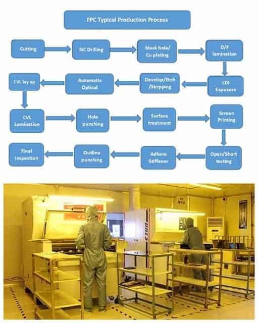
The typical workflow for assembling circuit boards includes the following key steps:
- PCB Fabrication – Producing bare PCBs via etching, drilling, etc.
- Stencil Creation – Laser-cut metal stencils for applying solder paste.
- Solder Paste Printing – Depositing paste over pads on the PCB through the stencil.
- Component Placement – Mounting components onto the PCB using pick and place machines.
- Reflow Soldering – Melting paste in an oven to form solder joints and adhere components.
- Inspection and Testing – Validating assembly quality and functionality.
- Conformal Coating – Applying protective coating over the assembled board.
Different methods and tools are used depending on the production scale, technology, and product requirements. We’ll explore PCB assembly steps in more detail throughout this guide.
Why Outsource vs. In-house Assembly?
For low-to-medium volume production, PCB assembly is commonly outsourced to a contract manufacturer. Reasons to outsource include:
- Cost savings – No investment in equipment and labor.
- Fast setup – Get started quickly without acquiring tools and expertise.
- Quality – Contract manufacturers have optimized assembly processes.
- Scalability – Production volumes can be flexibly adjusted.
- Turnkey service – Handle everything from procurement to shipping.
For higher production volumes, bringing assembly in-house allows:
- Tighter control – Over processes, quality, schedules, IP.
- Customization – Tailor processes to specific products.
- Cost savings – Lower per-unit cost at scale compared to outsourcing.
- Proximity – Faster feedback loops between engineering and production.
In-house also requires significant upfront and ongoing investments. The crossover point depends on economies of scale for a given product.
Tools for Circuit Board Assembly
Assembling PCBs requires an array of equipment and tools:
Solder Paste Printer
Prints solder paste on pads through a stencil for surface-mount components.
Pick and Place Machine
Automatically picks components and places them precisely onto the PCB.
Reflow Oven
Heats the assembly to melt solder paste, forming solder joints to attach components.
Wave Soldering Machine
Passing a PCB over a waver of molten solder attaches through-hole components.
Soldering Iron Station
For manual soldering, rework, repairs, and touch-up.
Conformal Coating Machine
Dispenses protective coating onto the assembled PCB.
Inspection Tools
Microscopes, x-ray, etc. to validate assembly quality.
Testing Equipment
Validates board functionality through in-circuit tests, flying probe tests, etc.
We will explore the key tools in more detail throughout this article.
Stencil Creation
The stencil is a thin metal sheet laser cut with apertures matching the solder pads on the PCB. It is aligned and placed onto the PCB. Solder paste is then squeegeed through the stencil openings, precisely printing paste onto the pads.
Typical stencil thickness is ~0.1mm. Stainless steel or nickel alloys are commonly used.
An adhesive-backed polyimide film added to the bottom side improves handling and prolongs stencil life.
The inner walls can have an electro-polished finish to reduce abrasion of the solder paste.
The stencil layout is generated based on the PCB design and component package footprints.
Laser cutting provides precision down to at least 0.1mm features. Chemical etching can also be used to manufacture stencils.
Stencils are specific to each PCB design and must be fabricated for each new assembly.
Solder Paste Printing Process
Solder paste printing deposits solder paste onto the PCB pads through the stencil apertures.
Typical solder paste consists of fine solder alloy particles suspended in flux and binding agents.
The main steps are:
- Dispense solder paste along one edge of the stencil.
- Use a squeegee blade to sweep the paste across the stencil, forcing it through apertures onto the PCB.
- Carefully remove the stencil, leaving precise printed solder paste deposits.
The process is repeated for double-sided boards. The PCB then proceeds to component placement.
A fine mesh screen can wipe excess paste off the stencil after each print.
An automated printer handles paste dispensing, squeegeeing, separation, and inspection functions.
Solder Paste Printing – Key Considerations
- Aperture design – Size and shape must match pads, with no gaps or insufficient overlap.
- Print speed – Faster printing risks smearing, while too slow causes separation.
- Pressure – Must be calibrated between squeegee, stencil, and PCB.
- Paste volume – Deposited paste must suit part sizes, with minimal excess.
- Separation speed – Slow, steady stencil separation avoids smearing.
- Paste condition – Paste must have correct viscosity and avoid drying.
- Cleaning – Keep stencil and tools clean between prints.
- Inspection – Verify paste deposits after each print.
With careful setup and process control, printing achieves accurate, consistent paste application.
Automated Pick and Place Machine
Pick and place machines automatically populate PCB assemblies by mounting components onto pads.
Key subsystems include:
- Feeders – Tape, trays, sticks, etc. to supply components.
- Picking Head – Nozzle that picks up individual parts.
- Optical Recognition – Identifies part orientation and position.
- Motion Control – High precision X-Y gantries for positioning.
- Software – Translates placement instructions into motion paths.
The assembly sequence is:
- Machine picks the component from the feeder.
- Checks alignment and orientation using optics.
- Moves it over the placement location.
- Lowers and places onto solder paste deposits.
- Releases the component and retracts the nozzle.
Cycle rates reach 4-10 seconds per chip. Highly parallel heads can simultaneously place dozens of parts.
Component Placement Process
The picking and placing sequence requires careful setup and optimization:
- Feeders – Tape reels must match component dimensions and be oriented consistently.
- Nozzles – Type and size must suit part shapes and sizes.
- Lighting – Allows clear imaging of components for alignment.
- Calibration – All motion axes require precision calibration.
- Program – The placement sequence must avoid collisions and optimize efficiency.
- Parameters – Settings like speed, acceleration, nozzle vacuum must be tuned.
- Maintenance – Nozzles, optics, feeders, and moving parts require regular cleaning and upkeep.
For reliable automated assembly, every sub-process must be finely dialed in through testing and adjustment.
Reflow Soldering Process
Reflow soldering uses precisely controlled heat to melt solder paste and form reliable solder joints to attach components onto the PCB assembly.
There are two main reflow methods:
Convection Oven: Board is passed through different temperature zones to gradually heat all joints evenly above melting point.
Vapor Phase: Board is immersed into an inert liquid heated at the solder melting point to uniformly reflow all joints.
A typical reflow oven profile:<table> <tr> <td>Zone</td> <td>1 Preheat</td> <td>2 Thermal Soak</td> <td>3 Reflow</td> <td>4 Cool Down</td> </tr> <tr> <td>Temperature</td> <td>150-200°C</td> <td>200°C</td> <td>220-260°C</td> <td>Below 150°C</td> </tr> </table>
The peak temperature and time in reflow must be optimized based on the solder alloy to fully melt and wet joints without damaging components.
Reflow Soldering Key Factors
Key process factors for successful soldering:
- Temperature profile – Gradual preheat and rapid cool down.
- Peak temperature – Above the melting point of the solder alloy used.
- Reflow atmosphere – Typically nitrogen or air.
- Time above liquidus – 30-90 seconds. Too long can damage parts.
- Convection – Air flow to evenly heat the assembly.
- Board thermal mass – Can require profile adjustments.
- Paste volume and alloy – Must be matched to part sizes and metallurgy.
- Wetting – Solder fully coats the soldered surfaces.
- Cool down – Rapid to avoid recrystallization issues.
The many interdependent variables require extensive profiling to optimize the soldering process.
Wave Soldering Process
Wave soldering is used to solder through-hole component leads and pins by passing boards over a wave of molten solder.
The key steps are:
- Flux application – Flux cleans surfaces and promotes solder wetting.
- Preheating – Brings board to just below solder melting point.
- Wave contact – Bottom of board contacts wave, soldering exposed metal surfaces.
- Cool down – Excess solder is pulled off, leaving solder fillets solidifying in holes and around leads.
Nitrogen blanketing prevents solder oxidation. Different nozzle designs form laminar waves to control solder flow and turbulence.
Dual waves are commonly used – with separate fluxing and soldering waves.
Inspection and Testing
Multiple inspection and testing steps validate assembly quality:
- Visual inspection – Verify part presence and orientation, solder joints, markings, overall appearance.
- X-ray inspection – Looks for hidden defects like voids in solder joints.
- ICT – In-circuit test electrically checks each net on the board.
- Flying probe – Tests electrical nodes and continuity by probing test points.
- Functional testing – Validates actual PCB performance and functionality.
Automated optical inspection compares boards against a template to identify defects.
Combining testing methods provides a complete view of assembly quality and reliability.
Conformal Coating
Conformal coating is an optional protective material applied over the fully assembled PCB. Benefits include:
- Moisture resistance – Protects against shorting and corrosion.
- Insulation – Prevents bridging between traces and components.
- Chemical resistance – Protects from solvents, cleaners, and other contaminants.
- Mechanical stability – Dampens shocks and vibration.
- Fungus resistance – Inhibits growth in high humidity.
Common conformal coatings include acrylic, polyurethane, silicone, and parylene. Select based on operating environment.
Conformal coating does makes rework and repairs more difficult. Weigh tradeoffs for your product.
Key Factors in Circuit Board Assembly
Here are some of the most crucial factors that determine assembly quality:
- Solder paste – Matching alloy, particle size, and viscosity to parts.
- Stencil design – Aperture sizes, shapes, and layout optimized for parts.
- Component placement – Accuracy within 50 μm.
- Reflow profile – Time above liquidus and peak temperature sufficient to fully melt solder.
- Thermal management – Avoiding excess thermal stresses on components.
- Contamination control – Preventing introduction of dirt, grease, residue, etc.
- ESD control – Grounding and isolation to avoid electrostatic discharge damage.
- Variation management – Consistency across materials, machines, operators, and environment.
Every step and parameter must be under control to achieve robust, reliable PCB assembly.
Frequently Asked Questions
What are common SMT assembly defects and how can they be prevented?
Tombstoning, solder balls, bridges, voids, skew, etc. Follow guidelines on stencil design, paste volume, reflow profile, component handling to avoid defects.
How small of components can be assembled using SMT?
Assembling 01005 chips is common. With care, 008004 (0.2mm x 0.1mm) chips can be placed. The lower limit depends on pad spacing, accuracy, vision systems, etc.
What types of solder paste are available?
Common options: no-clean, water soluble, low residue, halide-free, different metal loads, and alloys like SAC305, Sn/Ag, Sn/Pb, etc. Match to process needs.
What conformal coatings can operate at high temperatures?
Silicone, parylene, and some polyurethanes and epoxies can withstand over 200°C. Ensure chemical compatibility at temperature.
How is rework performed on assembled boards?
Using hottest air tools, manual soldering irons, solder wick, flux, etc. Remove and replace damaged components. Take care to avoid collateral damage.
Conclusion
Achieving high-quality PCB assembly requires expertise across a wide range of processes from stencil creation through final conformal coating. Careful control of equipment, materials, and parameters enables assembling boards with maximum reliability and repeatability. While requiring upfront investments in tools and learning, bringing assembly in-house allows customizing the process for specific products and closely integrating prototype engineering with production.


0 Comments