Introduction
Prototype printed circuit boards (PCBs) are a vital step in validating the design and performance of new electronic products before committing to full-scale production. This article explores the prototyping and small-batch fabrication processes, capabilities, and technical factors to consider when developing prototype boards.
Overview of PCB Prototyping vs Production
PCB prototyping involves fabricating a small number of boards (typically 5-100) to test out a design concept and work through technical issues and design revisions. The focus is on fast turnaround, flexibility, and close supplier interactions.
In contrast, production PCB fabrication involves established, high-volume processes to manufacture thousands to millions of boards cost-effectively. The focus is on consistency, yield, and minimal defects.
PCB Prototype Fabrication Process
The fabrication process for prototype PCBs involves the following key steps:
Engineering Data Preparation
- Create schematics, layouts, Gerber files, bill of materials, assembly drawings, fabrication notes.
- Perform design rule checks that align with capabilities of the PCB supplier.
- Send Gerber files to supplier for design review and quoting.
Order Processing
- Confirm technical requirements, tolerances, delivery dates, pricing.
- Finalize order quantities needed for prototyping testing phases.
- Set up purchase orders with supplier based on quoting.
Fabrication
- Generate phototools from Gerber data.
- Pattern imaging using lithographic processes.
- Copper plating of traces based on imaged pattern.
- Etching to remove copper foil on unneeded areas.
- Automated optical inspection (AOI) for defects.
- Apply protective solder mask over traces.
- Screen print legend for designators.
- Plate board edges with gold or tin.
- Route/drill holes.
- Bevel and deburr boards.
- Perform electrical testing.
Shipment
- Ship finished boards in ESD packaging.
- Include test reports, AOI data, and documentation.
Key Prototype PCB Specifications
Some key specifications to define when ordering prototype boards:
Layers – Number of copper layers, either single, double, or multilayer. Complexity increases with more layers.
Board Size – Dimensions (length, width) and shape. Cutting panels to size adds cost.
Board Thickness – Standard thickness is 1.6mm. Thinner boards save costs but compromise durability.
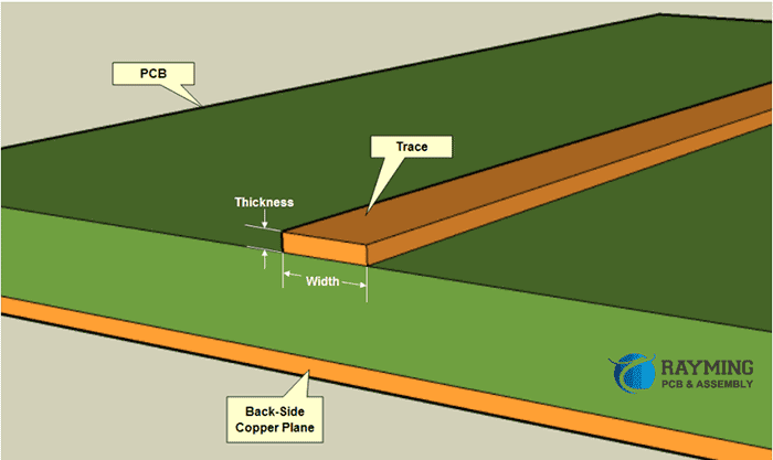
Trace/Space – Width and spacing of copper traces based on circuit density.
** Finishes** – Surface plating like HASL, immersion silver, ENIG, electoplating. Determines solderability.
Material – FR-4 glass epoxy is standard. Get RF/microwave boards use ceramic substrates.
Hole Size/Tolerance – Size of drilled holes for leads and vias. Tolerance impacts assembly fit.
Routing – Board shaping, cutouts, slots based on design needs and assembly.
Soldermask – Protective coating type (acrylic, epoxy) and color.
Silkscreen – Printed labels and identifiers. Define legend print quality needed.
Testing – Bare board electrical testing parameters to specify.
Design Considerations for Prototype PCBs
To streamline prototyping, keep these guidelines in mind when designing boards:
- Use larger trace/space widths for increased yield on small batches.
- Avoid tight component spacing and clearances to reduce fabrication scrap risk.
- Minimize high density interconnects which are prone to defects.
- Incorporate test points for easy probing during debugging.
- Ensure adequate hole sizes for hand soldering and rework.
- Only use as many layers as functionally required to limit costs.
- Modularize complex multilayer sections to enable incremental debugging.
- Include spare bypass capacitors, jumpers, and mounting holes for modifications.
- Define areas for design revisions using jumpers or zero-ohm resistors.
Comparing Prototype vs Production Fabrication
Prototyping vs production PCB fabrication differ in some key aspects:
| Parameter | Prototype PCB | Production PCB |
|---|---|---|
| Volume | Low, <100 units | High, thousands+ units |
| Lead Time | Short, 5-10 days | Long, 4+ weeks |
| Cost per board | High, $200-$1000+ | Low, <$10 at high volumes |
| Defect rate | Higher | Extremely low |
| Yields | Lower, 60-90% | 99%+ |
| Tooling | Minimal for small batches | Dedicated for volume |
| Testing | Functional validation | Automated electrical and in-circuit |
| Fixturing | Manual assembly | Dedicated SMT lines |
| Designrevision | Expected with each spin | Frozen after initial spins |
Best Practices for Prototype PCB Development
Here are some best practices when working on prototype boards:
- Do design reviews with your board shop before placing orders.
- Build in test points for debug and probing of signals.
- Simulate timing, power, thermal performance to catch issues early.
- Start with the simplest board layout that validates core functions.
- Design with future revisions in mind by planning component placement.
- Test key functions before full assembly by selectively populating boards.
- Perform incremental assembly, testing each stage before soldering more components.
- Inspect each populated board under a microscope before applying power.
Conclusion
Developing well-designed prototype boards lays the groundwork for transforming an electronics concept into a successful product. Planning PCB specifications, implementing design for prototyping guidelines, ordering small batch fabrication, and thorough validation testing allows for effective troubleshooting and design refinement before advancing to production. Partnering with an experienced prototype PCB shop accelerates the process from prototypes to mass production.
Frequently Asked Questions
How many prototype PCB revisions should be planned for a new design?
3-5 revisions is typical for more complex designs to incrementally debug and validate the electronics hardware. Budgeting for extra spins avoids delays.
What are the most common defects seen on prototype PCBs?
Shorts, opens, thin traces, under or over copper plating, poor holewall quality, mask/legend alignment issues, and handling damage are common.
Should every prototype board include all final features?
No, start with a minimal set of key functions to validate quickly. Additional features can be added in subsequent revisions once the core design is stable.
How many boards should be ordered for each prototype revision?
Start with 5 boards for simple proof of concept testing. Complex designs may need 10-25 boards to provide examples for diagnostics across multiple test configurations.
What are the signs that indicate a design is ready for high volume production?
It passed all functional and performance testing. All defects and issues from prototyping are resolved. Reliability is validated over thousands of test hours. Yield is high with the chosen supplier.


0 Comments