Introduction
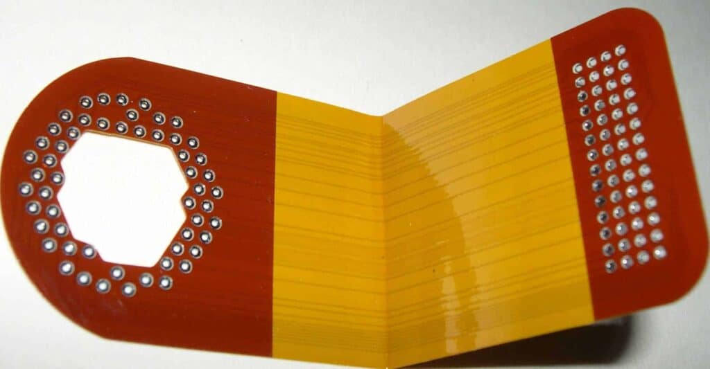
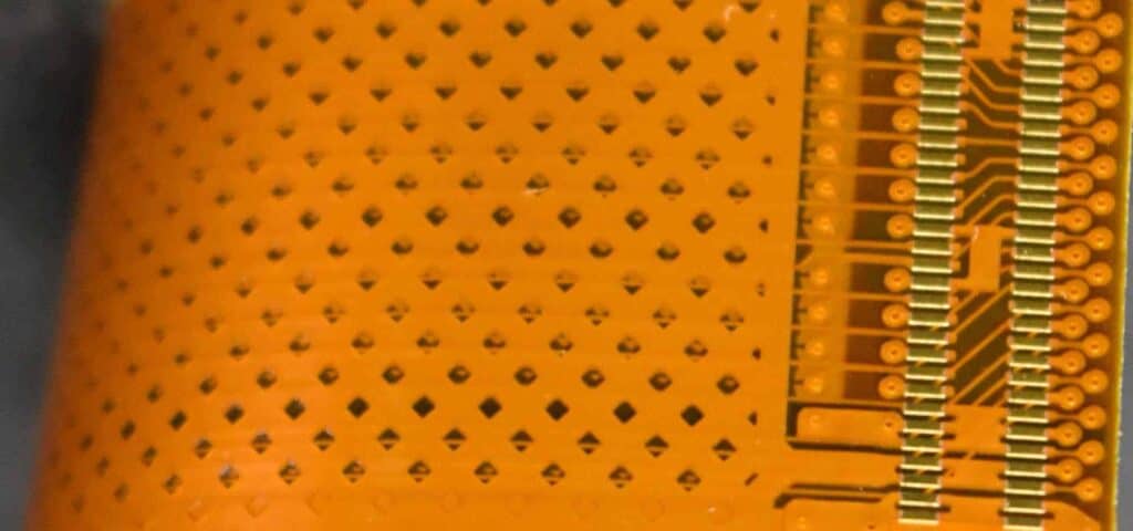
Printed circuit boards (PCBs) are an essential component of most electronic devices and products. A PCB provides the foundation for mounting and connecting electronic components using conductive copper traces etched from copper sheets laminated onto a non-conductive substrate.
When developing a new electronic device, prototypes PCBs allow designers and engineers to test the circuitry and functionality of a product during the design phase. Producing high-quality prototype PCBs correctly is crucial for verifying the viability of a product before committing to full-scale production.
This comprehensive guide provides key information on prototyping PCBs, including:
- Prototyping methods and capabilities
- PCB design software
- Generating fabrication files
- Selecting a prototype PCB manufacturer
- Lead times and costs
- Testing and validating boards
- Transitioning to production
Follow these best practices for procuring fast, affordable prototype PCBs that meet your requirements.
Overview of Prototype PCB Production Methods
Several methods exist for producing prototype printed circuit boards, each with their own advantages and drawbacks. Choosing the right prototyping technique depends on several factors:
- Quantity – Number of boards needed for testing.
- Lead Time – How quickly boards are needed.
- Capabilities – Layers, resolution, materials.
- Cost – Budget available for prototyping.
Here are some of the most common PCB prototype production methods:
Milling/Routing
A mechanical process that uses a specialized end mill to machine away copper from a blank PCB laminate to form the circuits.
Advantages: Fast turnaround, affordable for very low quantities.
Limitations: Limited to 2 layers. Lower resolution and tolerances.
Laser Direct Imaging (LDI)
Uses a laser to selectively ablate away unwanted copper to create the circuit traces.
Advantages: Fast turnaround, good features and tolerances.
Limitations: Limited to 2 layers. Lower quantities.
Photolithography
The traditional PCB production process of using photoresists, masks, light exposure, and etching to form copper traces.
Advantages: Allows high layer counts, good features, and tolerances.
Limitations: Slower and more expensive for low-volume prototyping.
Printed Electronics
Uses inkjet or aerosol jet printing to directly print conductive traces onto substrates.
Advantages: Very fast turnaround, low costs for simple single layer boards.
Limitations: Restricted to 1-2 layers. Lower conductivity and resolution.
PCB Design Software
To fabricate a custom printed circuit board, you first need to design the board layout using electronic design automation (EDA) software. PCB design software allows you to draw the circuits, place components, route connections, and define board layers.
Some of the most popular PCB design tools include:
- Altium Designer – High-end paid software with advanced features.
- Eagle – Popular inexpensive EDA software, now owned by Autodesk.
- KiCad – Free, open-source PCB design tool.
- OrCAD – Full suite of EDA tools from Cadence.
- Pad2Pad – Browser-based online PCB design application.
Key features to evaluate when selecting a PCB design system:
- Interface – Ease of use and layout capabilities.
- Libraries – Availability of component footprints and symbols.
- Features – DRC, annotation, autorouting, 3D viewer.
- Outputs – Gerber and drilling file generation.
- Cost – Purchase price and licensing options.
- Support – Documentation, tutorials, community.
Spending time learning a PCB design tool that fits your needs and budget will make prototyping circuit boards quicker and simpler.
Generating Fabrication Files
After completing the PCB layout, you need to export the necessary files used for board fabrication and assembly. Most PCB software can generate industry-standard outputs:
Gerber Files:
- Provide 2D vector images of each layer – top and bottom copper layers, solder mask, silkscreen, etc.
- Extended Gerber format includes attributes like aperture definitions.
- Review carefully to ensure all layers are present and contain the expected data.
Drill Files:
- NC drill files specify the size and location of all the holes to be drilled in the PCB.
- Excellon and Sieb & Meyer are common numeric control (NC) drilling formats.
- May include plated and non-plated holes.
Board Outline:
- Mechanical drawing or parameters defining the exact dimensions of the board profile.
- Important for panelization and edge treatments.
Component List:
- A bill of materials (BOM) listing all the parts references and values.
- Helps PCB assemblers populate the board correctly.
3D Models:
- Optional step file of a 3D render of the board and components.
- Used for design visualization and sometimes fabrication.
Carefully verify all output files before submitting to PCB prototype services. Any errors at this stage can lead to costly mistakes and production delays. Ask manufacturers about their preferred file formats.
Selecting a Prototype PCB Manufacturer
Choosing the right PCB manufacturer is key to achieving high-quality prototypes quickly and affordably. Here are key factors to consider:
Capabilities:
- Available PCB materials – FR-4, Rogers, polyimide, etc.
- Layer count – often up to 12 or more.
- Minimum track/space width – 5/5 mil or lower.
- Via sizes – laser-drilled microvias.
- Surface finishes – HASL, immersion silver, ENIG, etc.
- Solder mask and silkscreen color options.
- Lead-free assembly.
Production Time:
- Turnaround time from order to delivery.
- Rush and expedited options for fastest fabrication.
- Domestic vs. overseas manufacturing locations.
Order Quantities:
- Typical order sizes supported.
- Low quantity or single-piece prototyping.
- Discounts for larger volumes.
Quality:
- Experience producing high-mix, low-volume prototype boards.
- Quality certifications – ISO-9001, IPC, ITAR, etc.
- Reviews and customer references.
Customer Service:
- Technical assistance and engineering review.
- Communication and order tracking.
- Quote turnaround time.
- Support for design modifications.
Cost:
- Pricing may depend on size, layers, lead time, and quantity.
- Compare budget prototype services.
- Ask about additional fabrication options.
Research a variety of domestic and offshore PCB manufacturers to find one well-suited to your specific prototyping needs. Getting multiple quotes is advised.
Lead Times for Prototype PCB Production
The time required to fabricate printed circuit boards varies significantly depending on the manufacturer’s location and capabilities:
Domestic Prototype Services:
- As fast as 24 hours for basic boards.
- 1 to 4 days typical for more advanced PCBs.
- 5-10 day standard turnaround.
Low Cost Asian Fabrication:
- 10-15 days typical for standard production.
- 5-7 days for expedited fabrication.
- 2-3 days using fastest air freight.
Other Considerations for Lead Time:
- Queue time before production starts.
- Availability of specific PCB materials.
- Time for shipping and customs clearance.
- Delays for engineering reviews and design modifications.
- Potential delays due to order backlog.
Discuss expected lead times with your manufacturer and plan accordingly. Building in some buffer is advised when relying on prototype boards for development schedules.
Costs of Prototype PCB Production
Prototyping printed circuit boards in low quantities generally costs between $200 – $5000 depending on size, layer count, and manufacturing method used.
Typical PCB Prototype Cost Drivers:
- Number of layers – more layers increases cost.
- Board dimensions – larger boards cost more.
- Production time – rush fabrication has higher fees.
- Quantity – cost per board drops significantly at higher volumes.
- Advanced processes – HDI, controlled impedance, etc.
- Special materials – FR-4 alternatives, copper thickness.
- Hole plating – plated slots or vias increase cost.
- Finishes – immersion silver, gold, tin costs more than HASL.
- Testing – electrical testing and X-rays add cost.
- Stencils and assembly.
Cost Reduction Tips for Prototype PCBs:
- Use simplest design possible for prototype testing.
- Choose standard FR-4 material and 1 oz copper to start.
- Minimize board size and select panelization where suitable.
- Use least number of layers for prototyping needs.
- Avoid tight tolerances and stick to minimum 6/6 mil width/spacing.
- Specify budget solder mask and surface finishes.
- Compare prices from multiple fabricators.
Carefully evaluate PCB prototype cost quotes to avoid surprise charges. Ask lots of questions to understand what is included in manufacturer fees.
Testing and Validating Prototype Boards
Once prototype printed circuit boards are received, they must go through validation testing before integration into a product. Typical PCB tests include:
Visual Inspection:
- Check for any obvious defects in solder mask, silkscreen, or copper.
- Verify all layers match fabrication data files.
- Correct component footprints, markings, and polarity.
Dimensional Analysis:
- Use calipers and microscope to measure trace widths and clearances.
- Confirm via diameters and hole sizes.
- Check board thickness and outer dimensions.
Electrical Testing:
- Validate conductivity of traces and vias with multimeter probing.
- Perform continuity tests for short and open circuits.
- Verify insulation resistance.
- Test for impedance of critical traces if specified.
Functional Testing:
- Power up board and test operation of circuitry.
- Confirm I/O voltages and signal activity.
- Validate performance meets specifications.
Environmental Stress Screening (ESS):
- Expose PCB to thermal cycling, vibration, and power stressing.
- Verify boards still function normally afterwards.
Thoroughly vetting prototype PCBs reduces the chance of problems arising in production. Have a testing plan in place before receiving boards.
Transitioning Prototypes to Production
Once prototype printed circuit boards have passed all validation tests, they can transition to full-scale manufacture for end products.
Tips for ramping up to production:
- Design Reviews – Make any required hardware modifications based on prototyping feedback.
- Process Optimization – Tweak any layouts or fabrication steps to optimize yield and cost.
- Production Samples – Build small pilot runs first to confirm manufacturing line is ready.
- Quality Control – Define board acceptance, inspection, and test procedures.
- Supply Chain – Begin sourcing all production components and materials.
- Manufacturing – Audit and qualify volume PCB fabrication and assembly partners.
- Logistics – Establish distribution pipelines and inventory management.
With carefully engineered prototypes and a controlled ramp-up, PCB production will meet the quality, cost, and delivery demands of your product launch.
Frequently Asked Questions
What are the main advantages of prototyping PCBs?
The key benefits of building prototype printed circuit boards include:
- Validating the design functionality before large-scale manufacturing.
- Finding any issues early that require PCB layout modifications.
- Allowing testing of assembly processes and compatibility with enclosure designs.
- Enabling firmware development on actual PCB hardware.
- Reducing project development risk and preventing costly mistakes.
What design practices help reduce prototype PCB costs?
Tips for lowering prototype expenses while still meeting testing needs:
- Use the simplest board layout possible.
- Standardize on common FR-4 material and 1 oz copper builds.
- Avoid advanced processing steps like blind/buried vias.
- Relax tolerances to 6/6 mil line/space or greater.
- Stick to minimum number of layers required.
- Consider breakout boards for high-density sections.
- Review design to panelize multiple boards where possible.
How many prototype PCBs should be ordered?
The quantity depends on the required testing and how many units are needed for development. Typical starting points:
- 3-5 boards – Allows basic validation testing with some spares.
- 10 boards – Enough for full debugging and multiple assembly builds.
- 20+ boards – Allows thorough environmental stress screening.
- 50+ boards – Sufficient for field testing and demos.
Should every PCB prototype iteration go through full validation testing?
No, often simple 1-3 day “express runs” are used just to check design changes or component fits without extensive electrical testing.
Full validation testing is reserved for 5-10 day standard prototyping runs where boards go through complete environmental stress screening.
How do you handle PCB component sourcing for prototypes versus production?
For prototypes, reuse any components already on hand or use distributors for small quantities. For production, identify all parts needed and their ideal supply chain source for cost-optimized volume purchasing. Plan component sourcing in parallel with PCB fabrication to avoid delays.


0 Comments