
How to Make a Custom PCB: Everything You Need to Know Is Here
Introduction to Custom PCBs
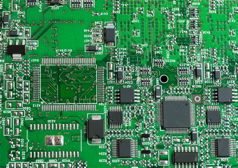
A custom printed circuit board (PCB) is a board that is specifically designed and manufactured to meet the unique requirements of a particular electronic device or project. Unlike generic PCBs, which are mass-produced and readily available, custom PCBs are tailored to the specific needs of the user, offering greater flexibility, functionality, and performance.
In this comprehensive guide, we will walk you through the process of creating a custom PCB, from the initial design phase to the final manufacturing and assembly stages. Whether you are an experienced electronics engineer or a hobbyist looking to create your first custom PCB, this article will provide you with all the information you need to get started.
Benefits of Using Custom PCBs
There are several advantages to using custom PCBs over generic, off-the-shelf boards:
-
Tailored Functionality: Custom PCBs are designed to meet the specific requirements of your project, ensuring that the board performs exactly as intended.
-
Optimized Layout: By designing your own PCB, you can optimize the component placement and trace routing for better signal integrity, reduced noise, and improved overall performance.
-
Cost-Effective: For larger production runs, custom PCBs can be more cost-effective than generic boards, as you only pay for the features and components you need.
-
Increased Reliability: Custom PCBs undergo rigorous testing and quality control measures to ensure that they meet the highest standards of reliability and durability.
-
Intellectual Property Protection: By using a custom PCB, you can safeguard your intellectual property and prevent competitors from easily copying your design.

The Custom PCB Design Process
The process of creating a custom PCB involves several key steps, each of which requires careful planning and execution.
Step 1: Schematic Design
The first step in creating a custom PCB is to develop a schematic diagram that represents the electrical connections between the various components of your circuit. This diagram serves as a blueprint for your PCB and helps ensure that all the necessary components are included and properly connected.
To create a schematic, you can use various electronic design automation (EDA) tools, such as:
- KiCad
- Eagle
- Altium Designer
- OrCAD
These tools allow you to place components, define their properties, and create the electrical connections between them. It is essential to double-check your schematic for errors before proceeding to the next step, as any mistakes at this stage can lead to costly revisions later on.
Step 2: Component Selection
Once your schematic is complete, the next step is to select the components that will be used on your custom PCB. This process involves choosing the appropriate components based on their electrical specifications, package size, and cost.
When selecting components, consider the following factors:
- Voltage and current ratings
- Power dissipation
- Tolerance
- Operating temperature range
- Availability and lead time
- Cost
It is also essential to ensure that the components you select are compatible with the manufacturing process you plan to use, such as surface mount technology (SMT) or through-hole mounting.
Step 3: PCB Layout Design
With your schematic and components in hand, you can now begin the PCB layout design process. This step involves arranging the components on the board and routing the electrical connections between them.
During the layout design process, consider the following best practices:
- Minimize trace lengths to reduce signal loss and interference
- Provide adequate spacing between components and traces to prevent short circuits
- Use appropriate trace widths based on the current carrying requirements
- Implement proper grounding and power distribution techniques
- Follow the manufacturer’s recommended footprint and layout guidelines for each component
EDA tools like those mentioned in Step 1 also offer PCB layout capabilities, allowing you to create a virtual representation of your board. These tools often include features such as auto-routing, design rule checking (DRC), and 3D visualization to help you optimize your layout and catch potential issues before manufacturing.
Step 4: Design Review and Verification
Before sending your custom PCB design for manufacturing, it is crucial to thoroughly review and verify your design to catch any errors or potential issues. This process involves several checks, including:
-
Design Rule Check (DRC): Ensures that your design meets the manufacturing specifications and design rules set by your chosen PCB fabricator.
-
Electrical Rule Check (ERC): Verifies that your schematic and PCB layout are electrically correct and free of shorts, open circuits, or other issues.
-
Bill of Materials (BOM) Review: Double-check that all the necessary components are included in your BOM and that their quantities, part numbers, and specifications are accurate.
-
Mechanical Check: Verify that your PCB fits within the required dimensions and that all the mounting holes, connectors, and other mechanical features are correctly placed.
-
Manufacturability Check: Consult with your PCB fabricator to ensure that your design can be manufactured using their processes and equipment.
Once you have completed these checks and made any necessary revisions, your custom PCB design is ready for manufacturing.

PCB Manufacturing Process
The manufacturing process for custom PCBs involves several steps, each of which is critical to ensuring the quality and reliability of the final product.
Step 1: PCB Fabrication
The first step in the manufacturing process is PCB fabrication, which involves creating the physical board based on your design files. This process typically includes the following sub-steps:
-
Film Generation: Your PCB design files are used to create a set of photographic films or digital images that will be used to transfer the circuit pattern onto the copper-clad board.
-
Copper Etching: The copper-clad board is coated with a light-sensitive resist, which is then exposed to UV light through the photographic films or digital images. The exposed areas of the resist are then removed, leaving behind a protective pattern that matches your circuit design. The board is then immersed in an etchant solution, which removes the unwanted copper, leaving behind the desired circuit pattern.
-
Drilling: Holes are drilled through the board to accommodate through-hole components and provide electrical connections between layers.
-
Plating: The drilled holes are plated with copper to provide electrical conductivity and ensure reliable connections between layers.
-
Solder Mask Application: A protective solder mask is applied to the board to prevent accidental short circuits and improve the board’s appearance. The solder mask is typically green, but other colors are available.
-
Silkscreen: A silkscreen layer is added to the board to provide labels, logos, and other identifying marks. This layer is typically white but can be any color.
Step 2: PCB Assembly
Once the bare PCB has been fabricated, the next step is to assemble the components onto the board. This process can be done using either through-hole or surface mount technology (SMT), depending on the types of components used and the design requirements.
For through-hole assembly, the components are inserted into the drilled holes and soldered in place. This process is typically done manually or using semi-automatic insertion machines.
For SMT assembly, the components are placed on the surface of the board and soldered using a reflow oven. This process is typically done using fully automatic pick-and-place machines, which can place hundreds of components per minute with high accuracy.
Step 3: Testing and Quality Control
After the PCB has been assembled, it undergoes a series of tests and quality control measures to ensure that it meets the required specifications and functions as intended. These tests may include:
-
Visual Inspection: A manual or automated visual inspection is performed to check for any visible defects, such as damaged components, solder bridges, or missing parts.
-
Automated Optical Inspection (AOI): An AOI machine uses high-resolution cameras and advanced image processing algorithms to detect any assembly defects or component placement errors.
-
X-Ray Inspection: For boards with hidden or inaccessible solder joints, such as ball grid array (BGA) packages, X-ray inspection may be used to verify the integrity of the connections.
-
In-Circuit Testing (ICT): An ICT machine uses a bed-of-nails fixture to make electrical contact with specific points on the board and verify the presence, orientation, and value of each component.
-
Functional Testing: The assembled board is powered on and tested to ensure that it performs the desired functions and meets the specified performance criteria.
Boards that pass these tests are then packaged and shipped to the customer, while those that fail are analyzed to determine the root cause of the issue and reworked or scrapped as necessary.

Choosing a PCB Manufacturer
Selecting the right PCB manufacturer is critical to ensuring the success of your custom PCB project. When evaluating potential manufacturers, consider the following factors:
-
Capabilities: Ensure that the manufacturer has the necessary equipment, processes, and expertise to fabricate and assemble your specific PCB design.
-
Quality: Look for manufacturers with a proven track record of producing high-quality PCBs and who adhere to industry standards such as IPC-A-600 and IPC-A-610.
-
Lead Time: Consider the manufacturer’s typical lead times and whether they can accommodate your project timeline.
-
Cost: Obtain quotes from multiple manufacturers and compare their prices, but be cautious of choosing the lowest bidder at the expense of quality or reliability.
-
Customer Support: Evaluate the manufacturer’s responsiveness, communication, and willingness to work with you to resolve any issues that may arise during the project.
By carefully selecting a reputable PCB manufacturer, you can ensure that your custom PCB project is completed on time, within budget, and to the highest standards of quality.
Designing for Manufacturability
To ensure that your custom PCB can be manufactured efficiently and cost-effectively, it is essential to design with manufacturability in mind. This involves considering the capabilities and limitations of the manufacturing process and making design choices that optimize the board for production.
Some key design for manufacturability (DFM) guidelines include:
-
Use standard component sizes and packages: Choose components that are readily available and compatible with the manufacturer’s assembly processes.
-
Provide adequate spacing between components: Ensure that there is enough space between components to allow for efficient placement and soldering.
-
Use appropriate trace widths and spacings: Follow the manufacturer’s design rules for minimum trace widths and spacings to ensure reliable electrical connections and prevent short circuits.
-
Avoid acute angles in traces: Use 45-degree angles or curved traces instead of 90-degree angles to improve signal integrity and reduce the risk of manufacturing defects.
-
Provide clear and accurate documentation: Include all the necessary design files, BOMs, and assembly instructions to minimize the risk of errors or misinterpretations during manufacturing.
By following these and other DFM guidelines, you can help ensure that your custom PCB is manufacturable, reliable, and cost-effective.
Common Pitfalls and How to Avoid Them
Creating a custom PCB can be a complex and challenging process, and there are several common pitfalls that can lead to delays, additional costs, or suboptimal performance. Here are some of the most common pitfalls and how to avoid them:
-
Incomplete or inaccurate documentation: Ensure that your design files, BOMs, and assembly instructions are complete, accurate, and up-to-date to prevent misinterpretations or errors during manufacturing.
-
Inadequate design review: Thoroughly review and verify your design before sending it for manufacturing to catch any errors or potential issues early in the process.
-
Ignoring manufacturability guidelines: Follow the manufacturer’s DFM guidelines and design rules to ensure that your board can be efficiently and reliably manufactured.
-
Rushing the design process: Allow sufficient time for the design, review, and verification processes to avoid costly mistakes or oversights.
-
Choosing the wrong components: Select components that are appropriate for your design requirements, budget, and availability to prevent issues with sourcing or compatibility.
-
Neglecting testing and quality control: Implement comprehensive testing and quality control measures to ensure that your custom PCB meets the required specifications and functions as intended.
By being aware of these common pitfalls and taking proactive steps to avoid them, you can help ensure the success of your custom PCB project.
Frequently Asked Questions (FAQ)
-
What is the difference between a custom PCB and a generic PCB?
A custom PCB is specifically designed and manufactured to meet the unique requirements of a particular electronic device or project, while a generic PCB is a mass-produced, off-the-shelf board that is designed to be used in a variety of applications. -
How long does it take to manufacture a custom PCB?
The lead time for manufacturing a custom PCB can vary depending on the complexity of the design, the chosen manufacturer, and the quantity ordered. Typical lead times range from a few days to several weeks, but expedited options may be available for an additional cost. -
What files do I need to provide to a PCB manufacturer?
To have your custom PCB manufactured, you typically need to provide the following files: - Gerber files: These are the industry-standard format for PCB design files and include information about the copper layers, solder mask, silkscreen, and drill holes.
- Drill files: These files specify the location, size, and type of drill holes required for your PCB.
- Bill of Materials (BOM): This is a list of all the components used on your PCB, including their quantities, part numbers, and specifications.
-
Assembly drawings: These drawings provide instructions for assembling the components onto the PCB, including their locations and orientations.
-
What are the most common PCB materials?
The most common materials used for PCB substrates are: - FR-4: A glass-reinforced epoxy laminate that is the most widely used material for PCBs due to its good electrical, mechanical, and thermal properties.
- Polyimide: A high-temperature, flexible material that is often used for applications requiring high reliability or resistance to harsh environments.
-
Aluminum: A metal-core material that is used for PCBs that require high thermal conductivity, such as those used in LED lighting or power electronics.
-
How can I reduce the cost of my custom PCB?
There are several ways to reduce the cost of your custom PCB: - Optimize your design for manufacturability by following DFM guidelines and using standard component sizes and packages.
- Choose a larger board size or panel size to take advantage of economies of scale.
- Reduce the number of layers in your PCB, if possible, to simplify the manufacturing process.
- Order larger quantities to benefit from volume discounts.
- Consider using a lower-cost PCB material, such as FR-4, if it meets your design requirements.
Conclusion
Creating a custom PCB can be a complex and challenging process, but by following the steps outlined in this guide and working with a reputable PCB manufacturer, you can bring your electronic projects to life with a high-quality, reliable, and cost-effective solution.
Remember to start with a well-designed schematic, select appropriate components, optimize your PCB layout for manufacturability, and thoroughly review and verify your design before sending it for manufacturing. By being aware of common pitfalls and taking proactive steps to avoid them, you can help ensure the success of your custom PCB project.
As you embark on your custom PCB journey, don’t hesitate to seek advice and support from experienced designers, manufacturers, and the wider electronics community. With the right knowledge, tools, and partners, you can unlock the full potential of custom PCBs and bring your innovative ideas to fruition.