
The Complete Guide to PCB Manufacturing
What is PCB Manufacturing?
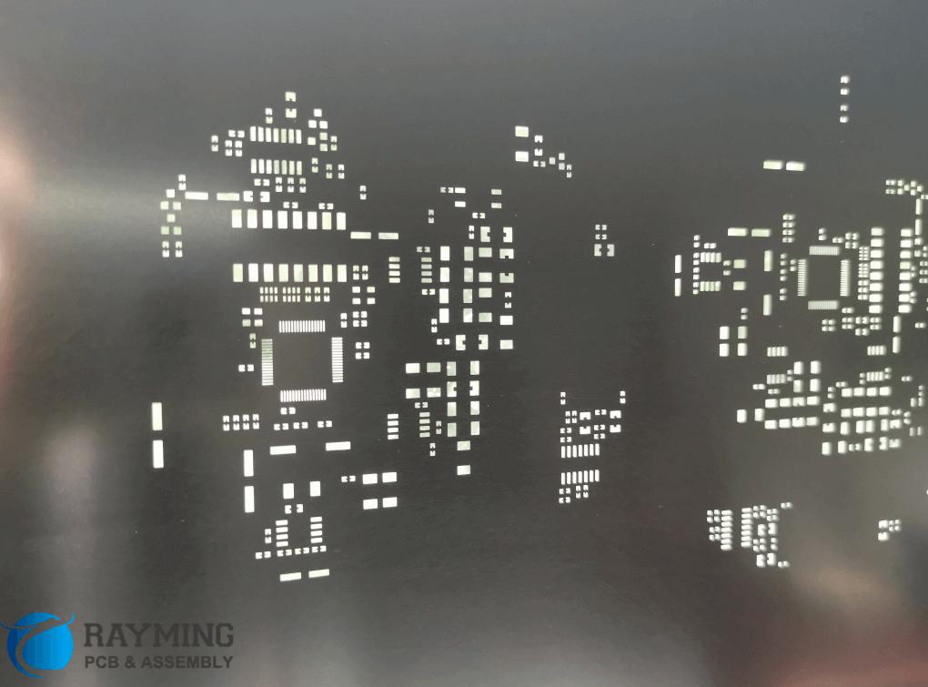
Printed circuit board (PCB) manufacturing is the process of designing and producing printed circuit boards from raw materials. A PCB serves as the basis for electronics that go into devices we use every day, from computers and phones to medical equipment and vehicles. The PCB manufacturing process involves taking a design for a circuit, etching and printing it onto a non-conductive substrate, and assembling the board with electronic components to create a functional electronic device.
PCB manufacturing involves precision and complex steps to transform raw materials into a finished circuit board. Understanding the PCB fabrication process helps designers and engineers optimize their board designs for manufacturability and cost-effectiveness. This guide provides a comprehensive overview of the PCB manufacturing process, from design to final assembly.
PCB Design and Layout
The first step in PCB fabrication is designing the board layout in CAD (computer-aided design) software. The PCB layout provides a blueprint for the manufacturer to follow during the fabrication process.
Good PCB design practices take into account:
- Component placement – Parts should be arranged logically for ease of assembly and maintenance. Grouping related components also helps reduce noise and crosstalk.
- Trace routing – Traces must make clean connections between pads while avoiding interference. Use 45- or 90-degree angles instead of curves.
- Stackup – Layer stackup, including dielectric materials and copper weights, affects cost and performance.
- High-speed design – Match trace impedances, provide shielding, and take transmission line effects into account.
- EMI/EMC – Follow good layout techniques to minimize electromagnetic interference (EMI) and susceptibility (EMC). Keep analog and digital circuits separated.
- Thermal considerations – Ensure adequate thermal relief for high-power components. Add thermal vias, pads, and planes as needed.
- Manufacturing rules – Follow fabrication house design rules for trace/space, hole sizes, etc.
- Testing points – Include test points to validate functionality during prototyping.
Following design for manufacturing (DFM) principles optimizes PCB layouts for reliability, assembly, and cost-effectiveness.
PCB Prototyping vs Production
Before going to full production, most PCB designs go through prototyping stages:
| Stage | Purpose | Volume | Lead Time |
|---|---|---|---|
| Breadboard | Functionality testing | 1 | Less than a day |
| Stripboard | Semi-permanent soldered prototype | 1-10 | 1-3 days |
| Manhattan style | First PCB prototyping | 1-10 | 1-3 days |
| 2-Layer PCB | Test manufacturing process | 10-100 | 1-2 weeks |
| 4+ Layer PCB | Pre-production validation | 100-1,000 | 2-4 weeks |
| Full Production | Go to market with product | 1,000+ | 4-6 weeks |
Prototyping helps confirm the design works and manufactures well before committing to a production run. As volumes increase, so does complexity, lead times, and costs.
PCB Fabrication Process Steps
PCB fabrication involves many complex chemical processes and machining operations. Here are the key steps in manufacturing a printed circuit board:
1. Base Material Selection
- Substrate – Common materials like FR-4, CEM-3, polyimide, etc. Determine mechanical, electrical and thermal properties.
- Copper foil – 1/2 to 2 oz thicknesses. Copper carries current between pads and traces.
- Dielectric layers – Core, prepreg, and other laminates. Provide insulation between copper layers.
2. Circuit Printing
- Film photolithography – A photomask is created from the PCB CAD files. The mask is used to optically transfer the circuit pattern onto a photosensitive chemical laminate on the copper layers.
- Etching – Exposed copper is etched away, leaving only the desired circuit pattern behind.
- Stripping – The remaining photoresist is chemically stripped off.
3. Lamination
- Sheets of core, prepreg, and copper foil are stacked and aligned.
- The stack is laminated with heat and pressure, bonding the layers together into a circuit board panel.
4. Hole Drilling
- Mechanical drilling – High speed CNC drills make holes for vias and component leads.
- Hole plating – Walls are plated with copper to electrically connect layers.
- Hole masking – Masks are applied to contain plating in holes.
5. Outer Layer Imaging
- Photolithography transfers the outer layer circuit images using solder masks and silkscreens.
6. Solder Mask & Silkscreen
- Solder mask – Epoxy layers prevent solder bridging between pads during assembly.
- Silkscreen – Prints component designators, logos, and other markings for identification.
7. Surface Finishes
- Immersion plating – Dips boards in solution to coat exposed copper with tin, gold, nickel, etc.
- ENEPIG – Electroless nickel, electroless palladium, immersion gold finish provides excellent wear resistance.
8. Panel Singulation
- Routed or punched to separate individual PCBs from the panel.
- Deburring removes rough edges from cut boards.
9. Quality Testing
- Electrical testing validates continuity, resistors, and function of circuits.
- Automated optical inspection looks for defects and contaminants.
- Impedance, signal integrity and other parameters may be tested.
This comprehensive fabrication process turns raw materials into fully functioning PCBs ready for assembly and installation. Variations exist for HDI, flex, and metal-core PCBs.
PCB Assembly Process
In addition to bare board fabrication, many manufacturers offer turn-key PCB assembly services. This streamlines the process of going from design to finished electronic product.
PCB assembly process steps include:
- SMT assembly – Surface mount components are precisely placed and soldered to pads on the board surface.
- Through-hole insertion – Leaded components are inserted into holes and soldered in place.
- Inspection and test – Boards are checked for correct assembly and functionality.
- Conformal coating – A protective coating may be applied to prevent environmental damage.
- Box build – The PCB is integrated and assembled together with other components into the final product enclosure.
By leveraging PCB assembly and box build services, product designers can minimize their hands-on manufacturing activities and focus more on design.
Factors that Influence PCB Cost
Many variables impact the cost of getting a PCB manufactured. Here are some key considerations:
| Factor | Effect on Cost |
|---|---|
| Board size | Larger boards use more materials. |
| Layer count | Each layer adds cost for materials, processing, drilling. |
| Advanced dielectrics | Low-loss, high-frequency, and exotic materials cost more than standard FR-4. |
| Tighter tolerances | High precision fabrication has more waste and lower yields. |
| Advanced finishes | ENIG, immersion silver, gold cost more than basic HASL. |
| Hole counts | More drilling time and plating chemicals. |
| Lead time | Rush orders add overtime and upcharge costs. |
| Low volume | Setting up for small runs increases cost per board. |
| Design complexity | High density interconnects require advanced processes. |
| Certifications | Military, aerospace, medical, etc. add testing and paperwork. |
| Offshore vs domestic | Offshore PCB shops typically have lower prices. |
Working closely with your PCB manufacturer early in the design process helps optimize designs for cost-effectiveness as well as quality and reliability.
Choosing a PCB Manufacturer
With so many PCB manufacturers to choose from, here are key considerations when selecting a fabrication partner:
- Capabilities – Ensure they can manufacture the board spec needed (layers, materials, tolerances, etc.)
- Quality – Look for ISO certifications, view internal quality procedures.
- Volume – Match manufacturing capabilities and pricing to production volume needs.
- Lead times – Evaluate ability to deliver on schedule for prototyping or production.
- Location – Onshore provides supply chain simplification; offshore can reduce cost.
- Customer service – Responsive sales and engineering support.
- Tooling and data – Many offer free CAD software and design rule files.
- Testing capabilities – In-house electrical, functional testing services.
- Certifications – ITAR, military, aerospace, medical facilities as required.
- Assembly services – One-stop-shop for design, fabrication, and assembly.
Get multiple quotes, review company certifications and customer reviews, inspect facility pictures and capabilities deck when selecting among PCB manufacturers.
PCB Manufacturing Technologies and Trends
Some emerging technologies and trends shaping PCB fabrication include:
- HDI PCBs – Enable higher interconnect density with microvias and thinner circuitry. Used in advanced consumer electronics and IoT products.
- Flex and rigid-flex – Bendable PCBs open new possibilities in wearable and consumer goods.
- Additive processes – Additive fabrication like inkjet and aerosol printing reduce waste versus traditional etching.
- Advanced materials – Substrates with improved thermal and RF performance for high-speed circuits.
- Fine line/space – Line spacing getting down below 2 mil allows for ultra-dense circuitry.
- 5G communication – High frequency 5G is driving designs with matched impedances, tight tolerances, and signal integrity.
- AI and automation – Machine learning improves automation, inspection, and optimization of PCB fabrication.
- Miniaturization – Making boards and components smaller, smarter, and more power efficient.
- Improved DFM – Tools analyze manufacturability earlier in the design process.
PCB technology continues advancing to provide smaller, higher performance, and lower cost solutions.
Conclusion
PCB manufacturing transforms electronic designs into functioning circuit boards in a complex, highly precise process. Each fabrication step must be carefully controlled to produce quality boards ready for component assembly. Engineers work closely with manufacturers to optimize the layout and select the most appropriate materials and finishes for performance, reliability, and cost targets.
Trends in the industry are pushing toward miniaturization, higher densities, and improved design tools to automate more of the PCB fabrication and assembly process. As electronics become ubiquitous across more products and markets, PCB manufacturing will continue innovating to deliver this key enabling technology.
Frequently Asked Questions
What are the most common materials used in PCBs?
The most common PCB substrate material is FR-4, a flame retardant epoxy resin reinforced with woven fiberglass. This offers a good balance of performance, cost, and manufacturability. Higher frequency boards may use advanced dielectric materials like PTFE, polyimide, or ceramic-filled composites.
What methods are used to manufacture flex PCBs?
Flex PCBs use polyimide or other flexible polymer substrates. Photolithography defines the conductors which are etched or laser ablated. Components mount to flex PCBs with conductive epoxy or solder, then the boards can be dynamically flexed during use.
How accurate is PCB fabrication?
With modern manufacturing, PCB feature tolerances can reach ±5 microns (±0.2 mil) or tighter for etching, ±25 microns for hole diameters. PCB registration alignment accuracy is typically around 50 microns.
Can PCBs be manufactured without laminating layers together?
Yes, processes like inkjet printing allow additively building up PCBs layer by layer without bonding dielectric and copper foil sheets. This reduces waste but currently has limitations on features size, precision, and material compatibility.
What are some ways PCB designs can be optimized for manufacturability?
Guidelines like following design rules, allowing adequate trace spacing, providing thermal relief, using 45/90 degree angles, and minimizing vias can improve manufacturability. Simulation and DFM tools also help optimize the design.