
Introduction
A printed wiring assembly (PWA), also known as a printed circuit assembly (PCA), is an essential component of many electronic devices. It consists of a flat board made of fiberglass or other insulating material on which thin copper foil pathways or “traces” are printed or etched. Electronic components are then soldered onto the PWA to form a complete circuit.
PWAs provide several advantages over traditional point-to-point construction methods:
- More consistent quality and reliability of connections
- Greater density of components and connections
- Lower assembly costs and faster production
- Easier troubleshooting and servicing of circuits
In this comprehensive guide, we will cover everything you need to know about printed wiring assemblies including their design, materials, manufacturing processes, testing, defects and repair.
Design and Layout
The design and layout of a PWA is a complex process that requires expertise in electronics engineering and PCB design software. Some key considerations include:
- Component placement – Parts must be arranged logically for efficient routing while minimizing wire lengths and crossovers. High-speed or noise-sensitive components require careful placement.
- Routing – Traces must make the required electrical connections between pads while following path constraints. Features like planes, voids and vias affect routing.
- Stackup – Layer stack and materials must suit electrical, thermal, mechanical and cost requirements. More layers allow higher complexity and density.
- EMI/EMC – Minimizing electromagnetic interference (EMI) radiation or susceptibility requires careful design of planes, traces, components and shields.
- Thermal – Heat dissipation requirements and component temperatures guide thermal plane design and trace sizing.
- Testability – Including design-for-test structures like vias under BGAs or testpoints aids in testing and fault isolation.
For low volume or prototype PWAs, manual routing may be viable, but higher volume production requires specialized PCB layout software like Altium, Cadence Allegro, Mentor Xpedition, and Zuken CR-8000.
Materials and Construction
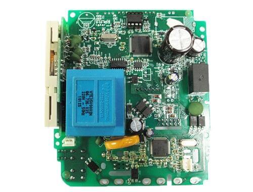
PWAs consist of three key material elements:
Substrate – The base PWA material is typically FR-4 fiberglass, but substrates like polyimide, PTFE, ceramic and metal core are used for demanding electrical, thermal or mechanical needs.
Conductors – Copper foil, usually 0.5-2 oz thickness, is patterned to form the conductive traces and pads. Some boards may use aluminum or silver conductors.
Solder mask – The solder mask is a polymer coating that insulates the copper traces, preventing solder bridges. Common colors are green and blue.
Other materials like silkscreen, finish plating, stiffeners and conformal coatings may be applied for marking, solderability, strength and protection. Components are attached via soldering, press-fit, conductive epoxy or other joining technologies.
| Substrate Materials | Properties |
|---|---|
| FR-4 | Standard glass-reinforced epoxy. Moderate cost. |
| CEM-1 | Woven fiberglass epoxy. Improved thermal performance. |
| Polyimide | High temp, flexible. Used in flex PCBs. |
| PTFE | Low loss, high frequency. Expensive. |
| Alumina ceramic | High frequency, excellent thermal, expensive. |
| Metal core | Metal baseplate for high power boards. |
Manufacturing Process
Printed wiring boards are fabricated using the following sequence of manufacturing processes:
- Substrate preparation – Cutting, drilling, cleaning, surface treatments.
- Conductor patterning – Additive or subtractive processes to form copper traces.
- Hole plating – Electrolytic copper plating to form conductive barrel walls.
- Solder mask application – Liquid photoimageable (LPI) coatings.
- Silkscreen printing – Ink printing for markings and legends.
- Surface finish – Organic solderability preservatives (OSPs), ENIG, immersion silver.
- Electrical testing – Bare board testing for shorts, opens and impedance.
- Assembly – Solder paste printing, component placement, reflow soldering.
- Inspection and test – Optical, x-ray and in-circuit testing.
Each process must be carefully controlled to meet requirements for line width, registration, impedance, solderability and reliability.
Defects and Fault Isolation
Despite best efforts, defects can occur on PWAs which require troubleshooting and repair:
- Shorts – Unintended connections between traces or pads. Visible or latent.
- Opens – Interruptions in intended connections due to nicks, ratsnests or broken traces.
- Solder defects – Insufficient solder, bridging, voiding or contamination.
- Component defects – Wrong, missing, damaged or counterfeit parts.
- Assembly errors – Miscallocated parts, reversed polarity.
Tools like optical inspection, x-ray, in-circuit testers, flying probe testers and automated optical inspection help isolate defects. If faults evade detection, diagnostic probing of nodes using an oscilloscope may be required.
Once located, many defects can be repaired by technicians using microsoldering techniques, conductive epoxy or jumper wires. For high-reliability systems, exhaustive testing before and after repair is mandatory.
Rework and Modification
In addition to repairing flaws, PWA rework is also done to:
- Replace obsolete parts or sub-assemblies with updated versions
- Upgrade functionality via new components in existing boards
- Correct design faults in prototype boards before finalization
Rework uses many of the same tools as PWA assembly like soldering irons, heat guns and solder paste. But specialized tools exist to improve efficiency and quality:
- Preheat plates for gentle, even heating of boards during desoldering
- Solder wick to remove solder for easy part removal
- Vacuum pickup tools to handle small components
- Precision soldering irons with fine tips for SMD work
- Adhesive gripping tools to hold parts in place during soldering
Careful process control is critical for rework to avoid collateral damage to boards or other components.boards
Testing and Inspection
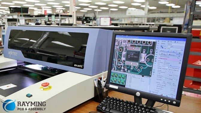
Testing is essential to confirm that PWAs function correctly before, during and after production:
- Design verification – Ensure simulated board performs to specifications.
- First article inspection – Complete evaluation of initial physical boards.
- In-process testing – Module tests during assembly process.
- ICT test – Uses test fixture to verify electrical performance.
- AOI – Automated optical inspection of solder joints.
- X-ray imaging – Reveals hidden solder defects.
- Flying probe – Tests continuity between points without fixturing.
- Boundary scan – Uses on-board JTAG to isolate faults.
- Functional test – Validates complete board behavior.
Rigorous testing reduces field failures and prevents defective products from reaching customers. Test coverage and diagnostics also provide feedback to improve manufacturing processes.
Applications
Printed wiring boards support virtually all modern electronics devices and systems:
- Consumer electronics – Phones, tablets, media devices, IoT.
- Computers – Motherboards, graphics cards, storage devices.
- Appliances – Microwaves, washing machines, smart home.
- Automotive – Engine controls, infotainment, instrument clusters.
- Industrial – PLCs, robotics, manufacturing, control systems.
- Medical – Imaging systems, monitors, pumps, analyzers.
- Military/aerospace – Avionics, guidance, communications, payloads.
Their compact size, reliable connectivity and support for SMD technology enable complex, feature-rich product designs. Continued innovation in PWAs underpins new generations of electronic products.
Future Outlook
The PWA industry continues to adapt to supply growing demands for sophisticated, affordable electronics:
- Miniaturization – Shrinking component sizes and finer line widths packing more functionality into smaller PWAs.
- High density interconnects (HDI) – Buildup processes allowing up to 30+ layers.
- Flex/rigid-flex – Bendable PWAs enhancing reliability in flexing environments.
- Embedded components – Capacitors, resistors and actives molded into the PWA substrate.
- Additive manufacturing – Printed electronics methods allow simplified PWA fabrication.
- Hybrid integration – Combining technologies like silicon interposers and chiplets.
With innovations in materials, design and manufacturing, the capabilities of printed circuit board technology will continue advancing.
Frequently Asked Questions
Q: What are some key differences between single-sided, double-sided, and multilayer PWAs?
A: Single-sided boards have conductors on one side only, double-sided adds a second external layer, while multilayer boards also incorporate internal conductive layers inside the PWA for increased interconnection capability. More layers allow greater component density and routing complexity.
Q: What are common surface finishes used on PWAs and why?
A: Common finishes include Hot Air Solder Leveling (HASL), Immersion Silver, Electroless Nickel Immersion Gold (ENIG) and Organic Solderability Preservatives (OSPs). These coatings protect exposed copper from oxidation and provide good solderability.
Q: How are components attached to PWAs?
A: Surface mount devices are attached by soldering to pads on the board surface. Through-hole components have wire leads inserted into plated holes and soldered. Press-fit and conductive epoxy attachment are also options.
Q: What causes tombstoning defects during SMD soldering?
A: Tombstoning happens when a component stands vertically due to uneven wetting forces during reflow soldering. Causes can include uneven termination metallization, misaligned parts or unbalanced paste volumes.
Q: What are common PWA acceptance and qualification tests?
A: Testing often includes netlist/artwork checks, in-circuit tests (ICT), x-rays for solder integrity, automated optical inspection (AOI), boundary scan, environmental stress tests, thermal cycling and vibration tests.