
Difference between Chemical and Plasma Etch Processes
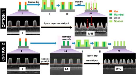
Introduction to Etch Processes
Etching is a crucial process in the fabrication of semiconductor devices and integrated circuits. It involves selectively removing material from a substrate to create desired patterns or structures. Two primary categories of etch processes are chemical etching and plasma etching. Each method has its own unique characteristics, advantages, and applications.
In this article, we will explore the differences between chemical and plasma etch processes, their mechanisms, and their roles in semiconductor manufacturing.
Chemical Etch Processes
Overview of Chemical Etching
Chemical etching, also known as wet etching, is a process that relies on liquid chemicals to remove material from a substrate. The substrate is immersed in an etchant solution, which selectively dissolves the exposed areas while leaving the masked regions intact. Chemical etching is an isotropic process, meaning it etches in all directions at the same rate, resulting in rounded or undercut profiles.
Mechanism of Chemical Etching
The mechanism of chemical etching involves three main steps:
- Transport of reactants: The etchant species are transported from the bulk solution to the substrate surface.
- Surface reaction: The etchant reacts with the substrate material, forming soluble products.
- Transport of products: The soluble products are transported away from the surface into the bulk solution.
The etch rate and selectivity of chemical etching depend on factors such as the composition of the etchant, temperature, agitation, and the nature of the substrate material.
Advantages of Chemical Etching
Chemical etching offers several advantages:
- Simplicity: Chemical etching is a relatively simple process that does not require complex equipment.
- Low cost: Wet etching is generally less expensive compared to plasma etching, as it does not require specialized vacuum systems or plasma generation equipment.
- High selectivity: Chemical etchants can be formulated to have high selectivity between different materials, allowing for precise pattern transfer.
- Batch processing: Multiple substrates can be etched simultaneously in a batch process, increasing throughput.
Disadvantages of Chemical Etching
Despite its advantages, chemical etching has some drawbacks:
- Isotropic etching: The isotropic nature of chemical etching can result in undercut profiles and limited resolution, especially for high aspect ratio features.
- Disposal of waste: Chemical etching generates liquid waste that needs to be properly treated and disposed of, which can be costly and environmentally challenging.
- Safety concerns: Some chemical etchants are hazardous and require careful handling and storage to ensure operator safety.

Plasma Etch Processes
Overview of Plasma Etching
Plasma etching, also known as dry etching, utilizes a plasma (an ionized gas) to remove material from a substrate. The substrate is placed in a vacuum chamber, and a plasma is generated by applying a strong electromagnetic field. The plasma consists of ions, electrons, and reactive species that interact with the substrate surface, causing material removal through physical and chemical mechanisms.
Mechanism of Plasma Etching
Plasma etching involves two main mechanisms:
- Physical etching: Energetic ions from the plasma bombard the substrate surface, physically sputtering away material. This mechanism is highly directional and can produce anisotropic profiles.
- Chemical etching: Reactive species in the plasma chemically react with the substrate material, forming volatile products that are pumped away. This mechanism is more isotropic and can provide high selectivity.
The balance between physical and chemical etching can be controlled by adjusting process parameters such as gas composition, pressure, power, and substrate temperature.
Types of Plasma Etching
There are several types of plasma etching techniques, each with its own characteristics and applications:
-
Reactive Ion Etching (RIE): RIE combines physical and chemical etching mechanisms. Ions are accelerated towards the substrate by an electric field, causing directional etching. Reactive gases are introduced to enhance chemical etching. RIE is widely used for anisotropic etching of various materials.
-
Inductively Coupled Plasma (ICP) Etching: ICP etching uses an inductively coupled plasma source to generate a high-density plasma. It allows for independent control of ion energy and plasma density, enabling high etch rates and excellent anisotropy. ICP etching is commonly used for deep etching of silicon and other materials.
-
Electron Cyclotron Resonance (ECR) Etching: ECR etching employs a microwave source and a magnetic field to create a high-density plasma. It operates at low pressures and provides good anisotropy and selectivity. ECR etching is suitable for etching materials that require low damage and high aspect ratios.
Advantages of Plasma Etching
Plasma etching offers several advantages over chemical etching:
- Anisotropic etching: Plasma etching can produce highly anisotropic profiles, enabling the fabrication of high aspect ratio features with vertical sidewalls.
- High resolution: The directional nature of plasma etching allows for better pattern transfer and higher resolution compared to chemical etching.
- Dry process: Plasma etching is a dry process that does not involve liquid chemicals, reducing the need for waste disposal and minimizing safety concerns.
- Versatility: Plasma etching can be used to etch a wide range of materials, including semiconductors, dielectrics, and metals.
Disadvantages of Plasma Etching
Despite its advantages, plasma etching also has some limitations:
- Complexity: Plasma etching systems are more complex and require specialized equipment, such as vacuum chambers, plasma sources, and gas delivery systems.
- Higher cost: Plasma etching equipment and operation can be more expensive compared to chemical etching.
- Plasma-induced damage: The energetic ions and reactive species in the plasma can cause surface damage, such as radiation damage or lattice defects, which may impact device performance.
- Etch rate uniformity: Achieving uniform etch rates across large substrates can be challenging due to plasma non-uniformity and loading effects.

Comparison of Chemical and Plasma Etch Processes
The following table summarizes the key differences between chemical and plasma etch processes:
| Characteristic | Chemical Etching | Plasma Etching |
|---|---|---|
| Etch Mechanism | Chemical dissolution | Physical and chemical removal |
| Etch Profile | Isotropic (rounded) | Anisotropic (vertical) |
| Etch Resolution | Limited by undercut | High, determined by plasma |
| Selectivity | High, based on chemistry | Moderate, depends on gas and power |
| Process Type | Wet (liquid) | Dry (gas) |
| Equipment | Simple, bath and chemicals | Complex, vacuum and plasma |
| Cost | Lower | Higher |
| Waste Disposal | Liquid waste, challenging | Gaseous byproducts, easier |
| Safety Concerns | Chemical handling | Plasma generation and handling |

Applications of Chemical and Plasma Etching
Both chemical and plasma etching have their own niche applications in semiconductor manufacturing:
Applications of Chemical Etching
- Bulk micromachining: Chemical etching is widely used for bulk micromachining of silicon, such as creating membranes, cavities, and channels in MEMS devices.
- Metallization patterning: Wet etching is commonly employed for patterning metal layers, such as aluminum or copper, in integrated circuits.
- Photoresist stripping: Chemical solvents are used to remove photoresist layers after lithography or as a cleaning step.
Applications of Plasma Etching
- Dielectric etching: Plasma etching is extensively used for etching dielectric materials, such as silicon dioxide and silicon nitride, in the fabrication of integrated circuits.
- Deep silicon etching: Deep Reactive Ion Etching (DRIE) is a plasma etching technique used for creating high aspect ratio structures in silicon, such as trenches, vias, and MEMS devices.
- Gate and contact etching: Plasma etching is employed for etching gate stacks and contact openings in CMOS technology.
- Photoresist ashing: Oxygen plasma is used to remove photoresist layers through a process called ashing, leaving behind a clean substrate surface.
Future Trends in Etch Processes
As semiconductor devices continue to shrink in size and increase in complexity, etch processes must evolve to meet the demanding requirements. Some future trends in etch processes include:
- Atomic Layer Etching (ALE): ALE is an emerging technique that enables precise, layer-by-layer removal of material with atomic-scale control. It combines sequential steps of surface modification and material removal, offering high selectivity and minimal damage.
- Cryogenic Etching: Cryogenic etching involves cooling the substrate to extremely low temperatures (e.g., -150°C) during the plasma etching process. This technique can enhance etch selectivity, reduce sidewall roughness, and minimize plasma-induced damage.
- Selective Etching: The development of highly selective etch processes that can remove specific materials while leaving others intact is crucial for advanced device fabrication. Selective etching can be achieved through the use of specialized chemistries or by exploiting differences in material properties.
- Plasma-Enhanced Atomic Layer Deposition (PEALD): PEALD is a technique that combines plasma processing with atomic layer deposition (ALD) to create conformal and ultrathin films. By integrating PEALD with plasma etching, it is possible to achieve precise patterning and selective deposition for advanced applications.
Conclusion
Chemical and plasma etch processes are essential techniques in semiconductor manufacturing, each with its own strengths and limitations. Chemical etching relies on liquid chemicals to selectively remove material, offering simplicity, low cost, and high selectivity. However, it is limited by its isotropic nature and the need for waste disposal. Plasma etching, on the other hand, utilizes a plasma to remove material through physical and chemical mechanisms, enabling anisotropic profiles, high resolution, and dry processing. However, it is more complex and expensive compared to chemical etching.
The choice between chemical and plasma etching depends on the specific application, material requirements, and desired etch characteristics. As semiconductor technology continues to advance, etch processes must evolve to meet the stringent demands of miniaturization and performance. Techniques such as atomic layer etching, cryogenic etching, selective etching, and plasma-enhanced atomic layer deposition are expected to play crucial roles in shaping the future of semiconductor fabrication.
Frequently Asked Questions (FAQ)
-
What is the main difference between chemical and plasma etching?
Chemical etching uses liquid chemicals to remove material isotropically, while plasma etching employs a plasma to remove material through physical and chemical mechanisms, resulting in anisotropic profiles. -
Which etching method is more suitable for high aspect ratio features?
Plasma etching, particularly techniques like Deep Reactive Ion Etching (DRIE), is more suitable for creating high aspect ratio features due to its anisotropic nature and ability to produce vertical sidewalls. -
Can chemical etching be used for etching dielectric materials?
While chemical etching can be used for etching some dielectric materials, plasma etching is more commonly employed for etching dielectrics like silicon dioxide and silicon nitride in integrated circuit fabrication. -
What are the safety concerns associated with chemical and plasma etching?
Chemical etching involves handling hazardous liquid chemicals, requiring proper safety measures and waste disposal. Plasma etching, on the other hand, involves the generation and handling of plasma, which requires precautions to avoid electrical hazards and exposure to radiation. -
What are some emerging trends in etch processes for advanced semiconductor manufacturing?
Some emerging trends in etch processes include atomic layer etching (ALE) for precise material removal, cryogenic etching for enhanced selectivity and reduced damage, selective etching for removing specific materials, and plasma-enhanced atomic layer deposition (PEALD) for conformal and ultrathin film deposition.