Introduction
SMT, or surface mount technology, is a method of assembling printed circuit boards (PCBs) that involves mounting electronic components directly onto the surface of the PCB without through-holes. SMT has revolutionized electronics manufacturing over the past few decades and is now the predominant method used for mass production of consumer electronics.
In this comprehensive guide, we will walk through the entire SMT assembly process step-by-step, from PCB design to soldering to inspection. We’ll also discuss the benefits of SMT, the equipment used, and key factors that impact quality and efficiency.
Overview of the SMT Assembly Process
The SMT assembly process can be broadly broken down into the following key stages:
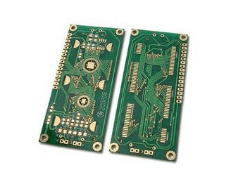
PCB Design and Fabrication
- PCB designed for SMT assembly with smaller pad/land sizes
- Panelized PCBs produced in large sheets for efficiency
- Solder mask added to prevent solder bridging
- Surface finishes like ENIG applied for solderability
SMT Stencil Creation
- Stencil designed and produced with cuts/apertures matching PCB pads
- Laser-cut or electroformed metal stencils commonly used
- Stencil aligned precisely to PCB for accurate paste deposit
SMT Paste Deposition
- Solder paste applied onto PCB pads through stencil apertures
- Reflow solder paste used with flux, spherical alloy powder
- Printing processes include screen printing, dispensers, jetting
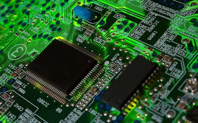
Component Placement
- Surface mount devices (SMDs) accurately placed onto solder paste
- High speed pick and place machines used for rapid placement
- Feeders supply components and camera vision checks placement
Reflow Soldering
- Entire loaded PCB assembly heated in oven to melt solder paste
- Solder joint formed with metallurgical bond between surfaces
- Different temperature profiles for lead-free vs. leaded solder
Post Solder Cleaning
- Cleaning removes flux residues from assembly after reflow
- Common options include water, solvents, saponifiers, laser
- Helps prevent issues like corrosion, dendrites, insulation resistance
Automated Optical Inspection
- Cameras and software check for defects after soldering
- Verify component placement, orientation, solder quality, bridging
- Helps catch issues early before functional testing
Functional Testing
- Application specific testing performed to validate operation
- Checks board functions, software, electronics meet specifications
- Issues detected late in process means higher rework costs
Conformal Coating
- Protective polymer materials applied to entire assembly
- Improves resistance to environment, prevents corrosion, leakage
- Dispensed as liquid or cured hard coat, selective or full coverage
This covers the overall sequence of major steps during a typical SMT assembly process. Next, we’ll go over these stages in more detail and discuss the options within each process.
Key Stages of the SMT Assembly Process
Below we take a deeper dive into the critical stages of SMT assembly:
PCB Design and Fabrication
The design of the printed circuit board is the first step in the SMT process flow. PCBs destined for SMT will be designed with smaller pad sizes to match the leads or balls on surface mount components. This includes metrics like pad width/length, shape, spacing, and mask opening.
Other SMT-specific design elements include:
- Panelization – PCBs arranged in larger sheets/panels for mass assembly
- Breakaway tabs – For separating individual boards after assembly
- Fiducials – Used by machines for alignment and placement
- Test/programming points – For validation after assembly
The PCB fabrication process also needs to produce a board optimized for SMT. This includes:
- Solder mask – Prevents solder bridging between pads during reflow
- Surface finish – ENIG, immersion tin, OSP coats pads for solderability
- Via protection – Tenting, plugging, or capping exposed vias
- High precision – Tight tolerances required for small components
SMT Stencil Creation
SMT stencils provide the pattern to accurately deposit solder paste onto the PCB pads during printing. Stencils are typically produced by laser cutting or etching processes.
Key considerations when creating SMT stencils:
- Design – Mirror image of PCB with apertures matched to pad sizes
- Type – Laser cut, electroform nickel, epoxy, chrome plated, others
- Thickness – Typically 0.1-0.15mm but varies based on needs
- Tolerances – Alignment features for precise alignment to PCB
- Draft angles – Help release paste from apertures during printing
- Surface – Polishing helps paste release; coatings reduce abrasion
High quality stencils correctly sized and aligned to the PCB are crucial for achieving good print transfer efficiency.
SMT Paste Deposition
Solder paste is applied onto the PCB pads through the apertures in the stencil. There are several solder paste deposition methods:
<b>Screen Printing</b>
- Squeegee pressed down and moved across stencil
- Forces paste through apertures onto pads below
- Most common method, fast and cost effective
<b>Stencil Printing</b>
- Similar to screen printing
- Uses enclosed stencil in a rigid frame, less flexible
- Good for high-mix, low-volume production
<b>Jetting</b>
- Heads jet tiny droplets of solder paste
- Non-contact, digitally-controlled deposition
- Lower waste compared to printing methods
- Slow process, high upfront system cost
<b>Dispensers</b>
- Deposit precise volumes of solder paste
- Typically used for rework, repair, or prototyping
- Slow, suited to low volume production
The primary solder paste considerations are metal powder type (SAC, SnPb, etc), powder size, flux type, and viscosity. These all impact printability, soldering performance, and quality.
Component Placement
Once solder paste is applied, the surface mount components must be accurately placed onto the wet paste deposits on the PCB pads.
High speed automated pick and place systems handle the component placement process. Key aspects include:
- Feeders – Supply components of various sizes/packages
- Pick heads – Use vacuum nozzle to pick components
- Camera – Aligns parts and inspects for defects or missing components
- Software – Programs component locations, pick/place sequence
- Speed – Modern systems place over >35,000 parts per hour
Precise component placement is critical for forming good solder joints later during reflow. Factors like positional accuracy and rotation impact quality.
Reflow Soldering
Reflow soldering melts the solder paste deposits to create permanent solder joints between the component leads/balls and PCB pads.
The reflow process involves:
- Heating – Typically done using convection ovens with IR heating
- Temperature profile – Time and temperature follows set ramps/soak/spikes
- Peak temperature – Melts solder paste, for lead-free usually 240-260°C
- Cool down – Fixed rate to avoid disturbances like tombstoning
- Atmosphere – Usually nitrogen or air/nitrogen mix
There are different reflow temperature profiles based on the solder alloy used. For example, lead-free SnAgCu solder has a higher melting point than traditional SnPb solder.
Reflow process parameters like time, temperature, and atmosphere must be tuned to achieve good wetting and formation of intermetallics.
Post Solder Cleaning
After soldering, cleaning processes remove residual flux and other contaminants from the PCB assembly. Common SMT cleaning methods:
- Aqueous – Use of water or water+detergent
- Solvent – Hydrocarbons, alcohol, or aqueous with saponifier
- Laser – Selective cleaning of local areas
- Plasma – Removes organics with ionized gas discharge
- Brushing – Physical scrubbing for difficult residues
Cleaning prevents issues like corrosion, electrical shorts, leakage currents, and dendrite growth during product operation.
Automated Optical Inspection (AOI)
AOI machines use cameras and software to automatically check assemblies for defects. Checks include:
- Correct component placement/orientation
- Solder joint quality – shorts, insufficient, excessive
- Solder bridging
- Missing or misaligned components
- Bill of materials (BOM) accuracy
- Board damage, markings, contamination
AOI provides critical feedback on assembly quality and helps catch defects early before functional testing.
Functional Testing
Functional testing validates that the populated board operates properly and meets all electrical and software specifications.
Common functional tests:
- In-circuit – Checks individual components
- Flying probe – Tests connectivity between points
- Bed of nails – Makes contact through test points
- System level – Validates entire system operation
- Software – Confirms firmware/programming
Failed boards can often be reworked depending on the issue. But the cost rises significantly at this late stage.
Conformal Coating
Conformal coatings are protective polymer materials applied to the full PCB assembly. Benefits include:
- Repels moisture, dust, chemicals
- Insulates conductive paths
- Strengthens solder joints against vibration, impact
- Reduces corrosion from environemental exposure
Coatings can be selectively applied to certain areas, or cover the entire assembly. Materials include acrylic, silicone, urethane, and parylene. Dispensing, spraying, or dip coating methods are used to apply the conformal coating.
This covers the key stages and considerations for each phase of the SMT assembly process flow. Next we’ll go over the benefits of SMT technology.
Benefits of SMT Assembly
There are several important benefits that make SMT the preferred assembly method for modern electronics:
- Smaller components – Higher component density with reduced weight and size
- Fewer defects – Lower solder joint failure versus through-hole assembly
- Automation – Enables high volume production with reduced labor
- Higher speed – Components can be placed faster than through-hole insertion
- Double-sided – Allows components on both sides of board
- Flexibility – Wide range of component sizes from 0201 chips to BGAs
- Testability – Small size lends itself to emerging methods like flying probe
- Reworkability – Individual components can be removed and replaced
SMT provides both technical advantages as well as significant cost savings compared to older through-hole assembly for most electronic products.
SMT Process Equipment
Specialized equipment is used at each stage of SMT assembly:
PCB fabrication
- Photolithography – Spin coaters, mask aligners, exposure units, developers
- Etching – Chemical etchers, vertical conveyorized spray etchers
- CAM – Computer aided manufacturing for panelization, routing
Solder paste printing
- Printer – For screen, stencil, or dispenser printing
- Stencils – Laser cutters, electroform etchers
- Solder paste – Mixers, dispensing and storage
- Printer setup – Microscopes, thickness gauges
Pick and place
- Machines – High speed chip shooters and multi-function
- Feeders – Tape, tray, stick, matrix tray, others
- Nozzles – Vacuum pick up tools for various components
- Vision systems – Aligners, barcode readers, OCR, defect inspection
Reflow
- Ovens – Convection, vapor phase, infrared, others
- Handlers – Linear and carousel type conveyor ovens
- Profiling – Thermocouples, dataloggers, thermal control
Inspection
- AOI – 2D and 3D automated optical inspection
- X-ray – Checks BGA joints and internal features
- Bond testing – Pull and shear testing machines
- ICT – Tests electrical connectivity and bed of nails
- Flying probe – Electrically probes points on a powered board
Rework
- Soldering irons – For manual component removal and replacement
- Hot gas stations – For site repair of BGAs
- Dispensing – Precise fluid deposit for rework and repair
Key Process Factors
There are a number of key factors that significantly impact the outcome, yield, and quality of the SMT assembly process:
- PCB design – Pad sizes, spacing, masks tailored to components
- Solder paste – Alloy properties, powder size, viscosity, flux
- Stencil – Quality, aperture design, thickness, alignment
- Component packaging – Tape and reel, trays, sticks
- Pick and place – Accuracy, precision, nozzles, feeders
- Reflow profile – Time, temperatures, ramps matched to paste
- Inspection – AOI programming, image quality, optics
- Operator training – Proper machine operation and maintenance
- Maintenance – Regular upkeep of printers, oven, AOI
- Traceability – Matching reels/batches through process
- Data management – Analysis tools to identify issues
- Contamination control – Proper storage, handling, ESD, etc
Tuning these parameters allows each process step to operate optimally and reliably produce good solder joints and quality boards. Deficiencies in any area can introduce defects and lower yields.
FQA
What are some key benefits of SMT assembly versus through-hole?
Some of the main benefits of SMT compared to through-hole assembly include:
- Smaller component sizes enable greater component density and smaller products
- Automated assembly is faster and lower labor than manual through-hole insertion
- SMT has fewer solder joint defects and fails due to improved process control
- Allows components on both sides of the PCB, not just one side
- SMT is flexible for a wide range of component sizes from 0201 chips up to large BGAs
- Easier rework of individual SMT components compared to desoldering through-hole parts
What is the typical solder alloy used for SMT assembly?
The most common solder alloy used for SMT assembly is the lead-free SAC alloy composed of tin, silver, and copper (SnAgCu). Typical ratios are 96.5% tin, 3% silver, and 0.5% copper. This alloy has favorable properties for SMT compared to the tin-lead solders previously used.
How does the stencil design impact SMT assembly?
The SMT stencil is critical for accurately transferring solder paste onto the PCB pads. The stencil design directly impacts quality:
- Aperture dimensions match PCB pads to deposit right volume
- Aperture pitch/spacing prevents bridging
- Thickness controls paste volume
- Draft angles aid paste release
- Surface polish reduces smearing and bridging
- Alignment features position stencil to PCB precisely
High precision laser cut stencils matched to PCB land patterns result in good solder paste printing.
What defects can AOI detect after SMT assembly?
Automated optical inspection after SMT assembly can detect defects like:
- Missing components
- Wrong components or orientation
- Insufficient or excessive solder
- Solder bridging between pads
- Poor co-planarity or tombstoning
- Damaged boards or markings
- BGA voiding or shorts under components
- Passive component skew/rotation
- Spacing violations
Programming AOI capabilities to maximally detect and classify these issues ensures quality boards.
How does process control impact SMT assembly yield?
Tight process control throughout SMT assembly is key to maximizing yield. Important factors:
- Consistent solder paste printing quality and volume
- Precision component placement accuracy and position
- Reflow profile optimized for paste and components
- Regular stencil and machine cleaning/maintenance
- Strict contamination controls
- Frequent inspection of solder paste, picks, and boards
- Data collection and trend analysis of defects
- Continuous improvement mindset
This level of process control, discipline, and data-driven efforts lead to reduced defects and higher yields.


0 Comments