
Recommended Points to Note in PCB Manufacturing
Introduction to PCB Manufacturing
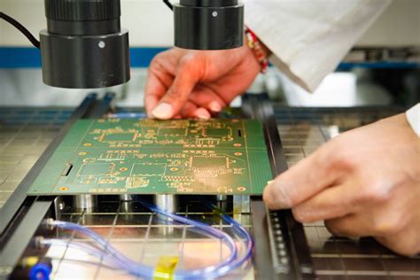
Printed Circuit Board (PCB) manufacturing is a complex process that involves several steps and considerations. To ensure the success of your PCB project, it is essential to understand the key points to note in PCB manufacturing. This article will provide an in-depth overview of the recommended points to note in PCB manufacturing, covering various aspects such as design, materials, fabrication, assembly, and testing.
PCB Design Considerations
Schematic Design
The first step in PCB manufacturing is creating a schematic design. This is a visual representation of the electronic components and their connections. When designing the schematic, consider the following points:
- Use a reliable PCB design software such as Altium Designer, Eagle, or KiCad
- Ensure that the schematic is clear, well-organized, and easy to read
- Use appropriate symbols for components and label them clearly
- Double-check the connections and ensure that they are correct
PCB Layout Design
Once the schematic design is complete, the next step is to create the PCB layout. This involves arranging the components on the board and routing the traces between them. Consider the following points when designing the PCB layout:
- Choose the appropriate board size and shape based on the application
- Determine the number of layers required based on the complexity of the circuit
- Place components strategically to minimize the length of traces and reduce signal interference
- Follow the manufacturer’s guidelines for minimum trace width, spacing, and hole size
- Use ground planes and power planes to reduce noise and improve signal integrity
- Consider the use of vias for connecting traces between layers
- Perform a design rule check (DRC) to ensure that the layout meets the manufacturing specifications

PCB Material Selection
PCB Substrate Materials
The choice of PCB substrate material depends on the application, operating environment, and budget. The most common PCB substrate materials are:
| Material | Description | Applications |
|---|---|---|
| FR-4 | Glass-reinforced epoxy laminate | General-purpose, low-cost |
| High Tg FR-4 | FR-4 with higher glass transition temperature | High-temperature, automotive, aerospace |
| Polyimide | High-temperature, flexible material | Aerospace, military, medical |
| Aluminum | Metal-based substrate for heat dissipation | High-power, LED lighting |
| Ceramic | High-temperature, high-frequency material | RF, microwave, high-power |
Copper Foil Thickness
The thickness of the copper foil on the PCB affects the current-carrying capacity and the impedance of the traces. The most common copper foil thicknesses are:
| Thickness (oz) | Thickness (µm) | Current Capacity (A/mm) |
|---|---|---|
| 0.5 | 17 | 0.3 |
| 1 | 35 | 0.6 |
| 2 | 70 | 1.2 |
| 3 | 105 | 1.8 |
| 4 | 140 | 2.4 |
Choose the appropriate copper foil thickness based on the current requirements and the desired trace impedance.
Solder Mask and Silkscreen
Solder mask is a protective layer applied to the PCB to prevent solder bridging and protect the copper traces from oxidation. Silkscreen is used to print text and symbols on the PCB for component identification and assembly instructions. Consider the following points when selecting solder mask and silkscreen:
- Choose a solder mask color that provides good contrast with the silkscreen
- Ensure that the solder mask apertures are correctly sized for the component pads
- Use a clear and legible font for the silkscreen
- Include polarity markings, component outlines, and pin numbers in the silkscreen

PCB Fabrication Process
PCB Etching
PCB etching is the process of removing unwanted copper from the PCB substrate to create the desired circuit pattern. The two main etching methods are:
- Chemical etching: Uses a chemical solution to dissolve the copper
- Plasma etching: Uses a plasma to remove the copper
Choose the appropriate etching method based on the complexity of the circuit, the desired feature size, and the production volume.
Drilling and Plating
After etching, the PCB needs to be drilled to create holes for through-hole components and vias. The holes are then plated with copper to create electrical connections between layers. Consider the following points when drilling and plating:
- Use the appropriate drill bit size for the hole diameter
- Ensure that the drill registration is accurate to avoid misaligned holes
- Use a plating thickness that meets the electrical and mechanical requirements
- Perform a visual inspection to ensure that the holes are clean and free of debris
Solder Mask and Silkscreen Application
The solder mask and silkscreen are applied to the PCB after drilling and plating. The solder mask is typically applied using a screen printing or photoimaging process, while the silkscreen is applied using a screen printing process. Consider the following points when applying solder mask and silkscreen:
- Ensure that the solder mask and silkscreen are correctly aligned with the copper traces and pads
- Use a solder mask thickness that provides adequate protection without affecting the component fit
- Cure the solder mask and silkscreen according to the manufacturer’s recommendations
- Perform a visual inspection to ensure that the solder mask and silkscreen are free of defects

PCB Assembly Process
Component Placement
Component placement is the process of positioning the electronic components on the PCB. This can be done manually or using automated pick-and-place machines. Consider the following points when placing components:
- Use a placement file that specifies the location and orientation of each component
- Ensure that the components are correctly aligned with the pads
- Use appropriate placement pressure and time to avoid damaging the components
- Perform a visual inspection to ensure that the components are correctly placed
Soldering
Soldering is the process of creating electrical connections between the components and the PCB. The two main soldering methods are:
- Wave soldering: Uses a molten solder wave to solder through-hole components
- Reflow soldering: Uses a reflow oven to solder surface-mount components
Choose the appropriate soldering method based on the component types and the production volume. Consider the following points when soldering:
- Use a solder paste with the correct alloy composition and particle size
- Ensure that the solder paste is correctly applied to the pads
- Use a solder mask to prevent solder bridging
- Control the soldering temperature and time to avoid component damage
- Perform a visual inspection to ensure that the solder joints are clean and free of defects
Cleaning and Inspection
After soldering, the PCB needs to be cleaned to remove flux residue and other contaminants. This can be done using a solvent or an aqueous cleaning process. Consider the following points when cleaning and inspecting the PCB:
- Use a cleaning process that is compatible with the PCB materials and components
- Ensure that the cleaning process removes all flux residue and contaminants
- Perform a visual inspection to ensure that the PCB is clean and free of defects
- Use an automated optical inspection (AOI) system to detect component placement and soldering defects
PCB Testing and Quality Control
Electrical Testing
Electrical testing is performed to ensure that the PCB functions as intended. This includes:
- Continuity testing: Verifies that there are no open or short circuits
- Insulation testing: Verifies that there are no leakage paths between conductors
- Functional testing: Verifies that the PCB performs the intended functions
Use appropriate test equipment and fixtures to perform the electrical testing. Consider the following points when performing electrical testing:
- Develop a comprehensive test plan that covers all the critical functions of the PCB
- Use test points and test pads to facilitate testing
- Perform the testing under the specified operating conditions
- Use statistical process control (SPC) to monitor the test results and identify trends
Environmental Testing
Environmental testing is performed to ensure that the PCB can withstand the expected operating conditions. This includes:
- Temperature cycling: Exposes the PCB to alternating high and low temperatures
- Humidity testing: Exposes the PCB to high humidity levels
- Vibration testing: Exposes the PCB to mechanical vibrations
- Shock testing: Exposes the PCB to sudden mechanical shocks
Use appropriate test equipment and chambers to perform the environmental testing. Consider the following points when performing environmental testing:
- Develop a comprehensive test plan that covers all the expected operating conditions
- Use accelerated testing methods to reduce the test time
- Monitor the PCB for any physical or functional degradation during the testing
- Use SPC to monitor the test results and identify trends
Quality Control and Documentation
Quality control and documentation are essential for ensuring the consistency and reliability of the PCB manufacturing process. Consider the following points when implementing quality control and documentation:
- Develop a quality management system (QMS) that complies with industry standards such as ISO 9001
- Use statistical process control (SPC) to monitor the key process parameters and identify trends
- Maintain detailed documentation of the PCB design, fabrication, assembly, and testing processes
- Use traceability systems to track the materials, components, and processes used for each PCB
- Perform regular audits and inspections to ensure that the processes are being followed correctly
- Provide training and certification for the personnel involved in the PCB manufacturing process
Frequently Asked Questions (FAQ)
-
What is the typical turnaround time for PCB manufacturing?
The turnaround time for PCB manufacturing depends on the complexity of the design, the materials used, and the production volume. Typical turnaround times range from 24 hours for simple prototypes to several weeks for complex, high-volume production runs. -
What are the most common PCB assembly defects?
The most common PCB assembly defects include: - Component misalignment or shifting
- Solder bridging or insufficient solder
- Tombstoning (component lifting off the pad)
- Reversed or missing components
-
Damaged or missing solder mask or silkscreen
-
How can I reduce the cost of PCB manufacturing?
To reduce the cost of PCB manufacturing, consider the following: - Optimize the PCB design for manufacturability
- Use standard materials and components whenever possible
- Minimize the number of layers and the board size
- Use larger trace widths and spacings to reduce the fabrication cost
-
Order in larger quantities to take advantage of volume discounts
-
What is the difference between wave soldering and reflow soldering?
Wave soldering is used for through-hole components and involves passing the PCB over a molten solder wave. Reflow soldering is used for surface-mount components and involves applying solder paste to the pads and heating the PCB in a reflow oven to melt the solder and create the connections. -
How can I ensure the reliability of my PCB?
To ensure the reliability of your PCB, consider the following: - Use high-quality materials and components
- Follow the design guidelines and best practices for PCB layout and routing
- Perform comprehensive electrical and environmental testing
- Implement a robust quality control and documentation system
- Work with a reputable PCB manufacturer with a track record of quality and reliability
Conclusion
PCB manufacturing is a complex process that requires careful consideration of numerous factors, from design and materials selection to fabrication, assembly, and testing. By following the recommended points outlined in this article, you can ensure the success of your PCB project and achieve the desired functionality, reliability, and cost-effectiveness.
Remember to work closely with your PCB manufacturer and communicate your requirements and expectations clearly. By establishing a strong partnership and maintaining open lines of communication, you can minimize the risk of errors and delays and achieve a high-quality PCB that meets your needs.