
What is Solder Beading?
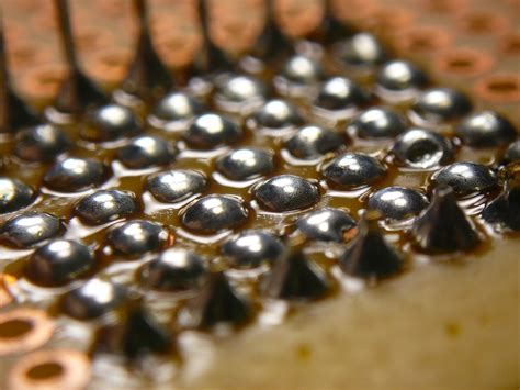
Overview of Solder Beading
Definition and Purpose
Solder beading, also known as solder bumping or dome soldering, is a method of depositing controlled amounts of solder onto specific areas of a PCB or electronic component. The main purpose of solder beading is to create robust and reliable electrical connections between components and the PCB substrate.
Advantages of Solder Beading
- Improved mechanical strength of solder joints
- Enhanced electrical conductivity and signal integrity
- Increased reliability and longevity of electronic assemblies
- Better resistance to thermal and mechanical stress
- Compatibility with various PCB surface finishes and component types
Solder Beading Process
Equipment and Materials
To perform solder beading, the following equipment and materials are typically required:
| Equipment/Material | Purpose |
|---|---|
| Soldering iron or solder station | Heating and melting the solder |
| Solder wire | Providing the solder material for beading |
| Flux | Promoting solder wetting and preventing oxidation |
| Tweezers or pick-and-place tool | Handling small components |
| Microscope or magnifying lens | Inspecting solder joints |
| Cleaning supplies (isopropyl alcohol, brushes) | Removing flux residue and cleaning the PCB |
Step-by-Step Procedure
-
Preparation: Clean the PCB and components to remove any contaminants or oxidation. Apply flux to the areas where solder beading will be performed.
-
Solder Application: Use a soldering iron with an appropriately sized tip to apply a controlled amount of solder onto the desired locations. The solder should form a dome-shaped bead upon cooling.
-
Inspection: Examine the solder beads under a microscope or magnifying lens to ensure proper shape, size, and uniformity. Check for any bridging, insufficient solder, or other defects.
-
Cleaning: Remove any excess flux residue using isopropyl alcohol and a clean brush or lint-free cloth. Ensure the PCB is clean and free from contaminants.
-
Testing: Perform necessary electrical tests to verify the functionality and reliability of the soldered connections.

Solder Bead Characteristics
Bead Shape and Size
The ideal solder bead should have a smooth, dome-shaped profile with a consistent size across all soldered locations. The size of the solder bead depends on factors such as the component package type, PCB pad dimensions, and the specific requirements of the electronic assembly.
Wetting and Adhesion
Proper wetting and adhesion of the solder bead to the PCB and component surfaces are crucial for achieving reliable electrical and mechanical connections. Factors that influence wetting and adhesion include:
- Surface cleanliness and oxidation
- Flux selection and application
- Solder alloy composition
- Soldering temperature and dwell time

Common Challenges and Solutions
Bridging and Solder Shorts
Bridging occurs when excess solder forms an unintended connection between adjacent pads or traces. To prevent bridging:
- Use a soldering iron with a fine tip for precise solder application
- Apply solder in controlled amounts
- Maintain proper spacing between components and PCB features
- Remove excess solder using solder wick or a desoldering tool
Insufficient or Excessive Solder
Insufficient solder can lead to weak connections and poor reliability, while excessive solder may cause bridging or poor bead shape. To ensure optimal solder amounts:
- Follow the recommended solder bead size guidelines for the specific component and PCB design
- Use solder wire with an appropriate diameter
- Maintain consistent soldering temperature and dwell time
- Inspect solder beads visually and rework if necessary
Flux Residue and Cleaning
Flux residue can lead to corrosion, electrical leakage, or poor adhesion if not properly cleaned. To address flux residue:
- Select a compatible flux for the solder alloy and PCB surface finish
- Use isopropyl alcohol or specialized cleaning solutions to remove flux residue
- Clean the PCB immediately after soldering to prevent the hardening of flux residue
- Verify cleanliness using visual inspection or contamination testing methods

Quality Control and Inspection
Visual Inspection Criteria
Visual inspection is a critical step in ensuring the quality of solder beads. Key criteria to consider during visual inspection include:
- Bead shape and size consistency
- Absence of bridging, insufficient solder, or excessive solder
- Proper wetting and adhesion to PCB and component surfaces
- Cleanliness and absence of flux residue or contaminants
Automated Inspection Techniques
For high-volume production or complex PCB assemblies, automated inspection techniques can be employed to enhance efficiency and accuracy. Common automated inspection methods include:
- Automated Optical Inspection (AOI): Uses computer vision algorithms to detect solder bead defects based on predefined criteria
- X-ray Inspection: Allows non-destructive inspection of solder joints, particularly for components with hidden or inaccessible solder beads
- Electrical Testing: Verifies the functionality and reliability of soldered connections through various electrical tests (e.g., continuity, resistance, insulation resistance)
Solder Beading Applications
Surface Mount Technology (SMT)
Solder beading is widely used in SMT assembly, where components are mounted directly onto the surface of the PCB. SMT components, such as chip resistors, capacitors, and integrated circuits, often require solder beading for reliable electrical and mechanical connections.
Through-Hole Technology (THT)
Although less common than in SMT, solder beading can also be applied in THT assembly. THT components with leads inserted through holes in the PCB can benefit from solder beading to enhance the strength and reliability of the solder joints.
Rework and Repair
Solder beading techniques are essential for rework and repair operations, where defective or damaged solder joints need to be corrected. Solder beading allows technicians to remove and replace components, repair solder bridges, and restore proper solder joint characteristics.
FAQ
What is the difference between solder beading and conventional soldering?
Solder beading focuses on creating raised, dome-shaped solder joints, while conventional soldering typically results in flat or concave solder joints. Solder beading provides enhanced mechanical strength, electrical conductivity, and reliability compared to conventional soldering.
Can solder beading be used on all types of PCBs and components?
Solder beading is compatible with most PCB surface finishes and component types, including SMT and THT. However, it is essential to consider the specific requirements of the PCB design, component package, and solder alloy to ensure optimal results.
How can I prevent bridging and solder shorts during solder beading?
To prevent bridging and solder shorts, use a soldering iron with a fine tip, apply solder in controlled amounts, maintain proper spacing between components and PCB features, and remove excess solder using solder wick or a desoldering tool.
What are the recommended cleaning methods for removing flux residue after solder beading?
Isopropyl alcohol or specialized cleaning solutions can be used to remove flux residue after solder beading. Clean the PCB immediately after soldering to prevent the hardening of flux residue, and verify cleanliness using visual inspection or contamination testing methods.
How can automated inspection techniques benefit solder beading quality control?
Automated inspection techniques, such as AOI, X-ray inspection, and electrical testing, can enhance the efficiency and accuracy of solder bead quality control. These methods help detect defects, verify functionality, and ensure the reliability of soldered connections in high-volume production or complex PCB assemblies.