
6 Points We need to Pay Attention to in Printed Circuit Assembly
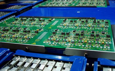
1. Component Selection and Placement
One of the most crucial aspects of PCB assembly is the selection and placement of components. This process involves choosing the right components based on the design specifications and placing them accurately on the PCB.
Factors to Consider in Component Selection
| Factor | Description |
|---|---|
| Functionality | The component must meet the required electrical and mechanical specifications. |
| Size | The component must fit within the allocated space on the PCB. |
| Cost | The component should be cost-effective without compromising quality. |
| Availability | The component should be readily available to avoid supply chain issues. |
Component Placement Techniques
- Manual placement: This method involves placing components by hand using tweezers or vacuum pens. It is suitable for low-volume production or prototyping.
- Pick-and-place machines: These automated machines are programmed to pick up components from feeders and place them accurately on the PCB. They are ideal for high-volume production.
2. Solder Paste Application
Solder paste is a mixture of tiny solder particles suspended in a flux medium. It is applied to the PCB pads before component placement to facilitate the soldering process.
Solder Paste Application Methods
| Method | Description |
|---|---|
| Stencil printing | A metal stencil with apertures corresponding to the PCB pads is used to apply solder paste evenly. |
| Dispensing | Solder paste is dispensed onto the pads using a syringe or a pneumatic dispenser. This method is suitable for small batches or rework. |
Factors Affecting Solder Paste Application
- Stencil design: The stencil aperture size and shape should match the PCB pad size and shape for optimal paste deposition.
- Solder paste properties: The solder paste’s viscosity, particle size, and flux activity should be suitable for the application.
- Printing parameters: The squeegee pressure, speed, and angle should be optimized to ensure even paste distribution.

3. Reflow Soldering
Reflow soldering is a process in which the PCB with components and solder paste is heated in an oven to melt the solder and form permanent connections.
Reflow Soldering Profile
A typical reflow soldering profile consists of four stages:
- Preheat: The PCB is gradually heated to activate the flux and remove solvents.
- Soak: The temperature is maintained to ensure even heat distribution and flux activation.
- Reflow: The temperature is raised above the solder’s melting point to allow solder joints to form.
- Cooling: The PCB is cooled down gradually to solidify the solder joints and prevent thermal shock.
Factors Affecting Reflow Soldering
- Oven temperature profile: The temperature profile should be optimized for the specific solder paste and components used.
- PCB design: The PCB layout, component density, and thermal mass affect the reflow process.
- Nitrogen atmosphere: Using nitrogen in the reflow oven can reduce oxidation and improve solder joint quality.

4. Inspection and Testing
After the soldering process, it is essential to inspect and test the assembled PCBs to ensure quality and reliability.
Inspection Methods
| Method | Description |
|---|---|
| Visual inspection | Manual or automated visual inspection is performed to check for visible defects such as solder bridges, missing components, or misaligned parts. |
| Automated optical inspection (AOI) | AOI systems use cameras and image processing algorithms to detect defects and compare the assembled PCB with the design data. |
| X-ray inspection | X-ray systems are used to inspect hidden solder joints, such as those under ball grid array (BGA) components. |
Testing Methods
- In-circuit testing (ICT): ICT involves using a bed-of-nails fixture to test individual components and their connections on the PCB.
- Functional testing: The assembled PCB is tested in its final application to verify its functionality and performance.
- Boundary scan testing: This method uses built-in test circuitry (JTAG) to test the interconnections between components on the PCB.

5. Rework and Repair
Despite best efforts, some assembled PCBs may require rework or repair due to defects or design changes.
Rework Techniques
- Desoldering: Defective components are removed using desoldering tools such as desoldering irons, hot air stations, or desoldering braid.
- Component replacement: New components are soldered in place of the removed ones, either manually or using a rework station.
Factors to Consider in Rework and Repair
- Thermal stress: Excessive heat during rework can damage the PCB or surrounding components.
- Electrostatic discharge (ESD): Proper ESD precautions should be taken to prevent damage to sensitive components.
- Skill level: Rework and repair require skilled operators to ensure quality and minimize further damage.
6. Documentation and Traceability
Maintaining proper documentation and traceability throughout the PCB assembly process is crucial for quality control, troubleshooting, and regulatory compliance.
Documentation
- Bill of materials (BOM): A comprehensive list of all components used in the assembly, including part numbers, quantities, and specifications.
- Assembly drawings: Detailed drawings showing the placement and orientation of components on the PCB.
- Work instructions: Step-by-step instructions for the assembly process, including any special requirements or precautions.
Traceability
- Lot tracking: Recording the lot numbers of components and materials used in each assembly for traceability in case of issues.
- Serialization: Assigning unique serial numbers to each assembled PCB for identification and tracking.
- Date coding: Marking the assembly date on the PCB or packaging for reference.
Frequently Asked Questions (FAQ)
1. What is the difference between through-hole and surface-mount technology (SMT) in PCB assembly?
Through-hole technology involves inserting component leads through holes drilled in the PCB and soldering them on the opposite side. SMT components are placed directly on the PCB surface and soldered using a reflow process. SMT allows for smaller components and higher density assembly compared to through-hole technology.
2. What are some common defects encountered in PCB assembly?
Common defects in PCB assembly include:
– Solder bridges: Unintended connections between adjacent pads or traces.
– Cold solder joints: Weak or incomplete solder connections due to insufficient heat or poor wetting.
– Tombstoning: When a small two-terminal component stands up on one end due to uneven heating or pad design.
– Component misalignment: When components are placed incorrectly or shifted during the reflow process.
3. How can I prevent electrostatic discharge (ESD) damage during PCB assembly?
To prevent ESD damage, follow these best practices:
– Use ESD-safe workstations, including grounded mats, wrist straps, and dissipative flooring.
– Handle sensitive components using ESD-safe tweezers or vacuum pens.
– Store components and assemblies in ESD-safe packaging when not in use.
– Train personnel in ESD awareness and proper handling techniques.
4. What is the purpose of using a nitrogen atmosphere in the reflow soldering process?
A nitrogen atmosphere in the reflow oven helps to reduce oxidation on the solder joints during the soldering process. Oxidation can lead to poor wetting, weak joints, and decreased reliability. By using nitrogen to displace oxygen in the oven, the solder joint quality and appearance are improved.
5. How can I optimize the reflow soldering profile for my specific PCB assembly?
To optimize the reflow soldering profile, consider the following factors:
– Solder paste specifications: Consult the solder paste manufacturer’s recommended temperature profile.
– Component characteristics: Consider the heat sensitivity and thermal mass of the components used.
– PCB design: Take into account the PCB thickness, layer count, and copper coverage.
– Oven capabilities: Ensure that your reflow oven can accurately control the temperature and maintain the desired profile.
Start with a generic profile based on the solder paste type and gradually fine-tune it through a series of test runs and evaluations. Monitor the solder joint quality, component integrity, and overall assembly reliability to determine the optimal profile for your specific PCB assembly.
In conclusion, paying attention to these six critical points in printed circuit assembly – component selection and placement, solder paste application, reflow soldering, inspection and testing, rework and repair, and documentation and traceability – can help ensure high-quality, reliable, and cost-effective results. By understanding and optimizing each aspect of the assembly process, manufacturers can produce PCBs that meet the ever-increasing demands of modern electronic devices.