
How to Panelise Round Shaped PCB’s
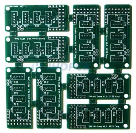
Introduction to PCB Panelization
PCB panelization is the process of combining multiple printed circuit board (PCB) designs onto a single panel for manufacturing. This technique is commonly used to increase production efficiency and reduce costs. By placing multiple PCBs on a single panel, manufacturers can minimize material waste, reduce setup time, and streamline the assembly process.
When it comes to panelizing round-shaped PCBs, there are several factors to consider to ensure optimal results. In this article, we will explore the various techniques, guidelines, and best practices for panelizing round-shaped PCBs effectively.
Understanding Round-Shaped PCBs
Round-shaped PCBs are becoming increasingly popular in various applications, such as wearable devices, IoT sensors, and industrial equipment. These PCBs offer unique advantages, including:
- Compact size and lightweight design
- Improved aesthetics and visual appeal
- Enhanced flexibility and durability
- Reduced sharp edges and improved safety
However, panelizing round-shaped PCBs presents its own set of challenges compared to traditional rectangular PCBs. The circular shape requires careful consideration of panel layout, routing, and manufacturing constraints.

Techniques for Panelizing Round-Shaped PCBs
1. Tab Routing
Tab routing is a common technique used for panelizing round-shaped PCBs. In this method, small tabs are created between the individual PCBs on the panel. These tabs act as breakaway points, allowing the PCBs to be easily separated after manufacturing. The tabs are typically made of the same material as the PCB substrate and are designed to be strong enough to hold the PCBs in place during fabrication and assembly.
When implementing tab routing for round-shaped PCBs, consider the following guidelines:
- Tab width: The width of the tabs should be sufficient to provide structural integrity during manufacturing but narrow enough to allow easy separation. A common tab width range is 0.5mm to 1.5mm.
- Tab placement: Position the tabs evenly around the perimeter of the round-shaped PCBs to ensure balanced support and minimize panel warping.
- Tab number: The number of tabs required depends on the size and weight of the PCBs. Generally, a minimum of three tabs is recommended for stable support.
2. V-Scoring
V-scoring is another technique used for panelizing round-shaped PCBs. In this method, V-shaped grooves are cut into the panel material between the individual PCBs. These grooves create weak points that allow the PCBs to be easily snapped apart after manufacturing. V-scoring is typically performed using a specialized cutting tool or laser.
When applying V-scoring to round-shaped PCBs, consider the following:
- Groove depth: The depth of the V-shaped grooves should be carefully controlled to ensure easy separation without compromising the structural integrity of the PCBs. A typical groove depth is between 30% to 50% of the panel thickness.
- Groove placement: Position the V-shaped grooves strategically around the perimeter of the round-shaped PCBs to facilitate clean and accurate separation.
- Groove angle: The angle of the V-shaped grooves can impact the separation process. A typical angle range is between 30° to 60°, with 45° being a common choice.
3. Perforated Routing
Perforated routing involves creating a series of small, closely spaced holes along the outlines of the individual PCBs on the panel. These perforations weaken the material, allowing the PCBs to be easily separated by breaking along the perforated lines. Perforated routing can be achieved using a CNC machine or a specialized perforating tool.
When employing perforated routing for round-shaped PCBs, consider the following:
- Hole size and spacing: The size and spacing of the perforations should be optimized to ensure easy separation without compromising the structural integrity of the PCBs. Typical hole diameters range from 0.5mm to 1mm, with a spacing of 1mm to 2mm between holes.
- Hole placement: Position the perforations evenly around the perimeter of the round-shaped PCBs to facilitate clean and accurate separation.
- Hole shape: Circular or oval-shaped perforations are commonly used, as they provide smooth edges and minimize stress concentrations.

Panel Layout Considerations
When panelizing round-shaped PCBs, the panel layout plays a crucial role in optimizing manufacturing efficiency and minimizing material waste. Consider the following factors when designing the panel layout:
1. PCB orientation and Spacing
- Arrange the round-shaped PCBs on the panel in a way that maximizes material utilization and minimizes waste.
- Ensure sufficient spacing between the PCBs to accommodate the chosen panelization technique (tab routing, V-scoring, or perforated routing) and allow for proper separation.
- Consider the placement of Fiducial Marks, tooling holes, and other panel features to aid in manufacturing alignment and assembly.
2. Panel Size and Material
- Select an appropriate panel size that accommodates the desired number of round-shaped PCBs while considering manufacturing constraints and equipment limitations.
- Choose a panel material that is compatible with the PCB substrate and meets the required electrical, mechanical, and environmental properties.
- Consider the panel thickness and its impact on the panelization technique, as thicker panels may require adjustments to tab width, V-groove depth, or perforation size.
3. Routing and Clearances
- Ensure adequate clearance between the round-shaped PCBs and the panel edges to prevent damage during handling and manufacturing.
- Consider the routing requirements for the panelization technique, such as tab placement, V-groove positioning, or perforation spacing.
- Verify that the routing paths do not interfere with any critical components or features on the PCBs.

Manufacturing Considerations
When panelizing round-shaped PCBs, it is essential to collaborate closely with the PCB manufacturer to ensure successful fabrication and assembly. Consider the following manufacturing aspects:
1. Equipment Capabilities
- Discuss the panelization requirements with the manufacturer and verify that their equipment can accommodate the chosen technique (tab routing, V-scoring, or perforated routing) for round-shaped PCBs.
- Ensure that the manufacturer has experience working with round-shaped PCBs and can meet the required tolerances and specifications.
2. Material Handling
- Communicate any specific handling requirements for the round-shaped PCBs, such as electrostatic discharge (ESD) protection or special packaging needs.
- Verify that the manufacturer has proper procedures in place for handling and storing the panelized PCBs to prevent damage or contamination.
3. Testing and Inspection
- Discuss the testing and inspection requirements for the panelized round-shaped PCBs with the manufacturer.
- Ensure that the manufacturer has adequate quality control measures in place to verify the integrity of the panelization, including visual inspection, electrical testing, and mechanical testing as needed.
Best Practices for Panelizing Round-Shaped PCBs
To achieve optimal results when panelizing round-shaped PCBs, consider the following best practices:
- Collaborate closely with the PCB manufacturer throughout the panelization process to ensure clear communication and alignment of expectations.
- Provide detailed documentation, including panel layouts, dimensions, and specifications, to minimize errors and ambiguity.
- Conduct thorough design reviews and simulations to validate the panelization approach and identify potential issues before manufacturing.
- Incorporate appropriate panel markings, such as part numbers, revision codes, and orientation indicators, to facilitate accurate assembly and traceability.
- Consider the use of automated assembly processes, such as pick-and-place machines or robotic systems, to improve efficiency and accuracy when working with panelized round-shaped PCBs.
- Perform rigorous testing and inspection of the panelized PCBs to ensure they meet the required quality standards and functional requirements.
- Continuously monitor and optimize the panelization process based on feedback from manufacturing, assembly, and end-use performance to drive continuous improvement.
Frequently Asked Questions (FAQ)
-
What is PCB panelization, and why is it important for round-shaped PCBs?
PCB panelization is the process of combining multiple PCB designs onto a single panel for manufacturing. It is particularly important for round-shaped PCBs as it helps increase production efficiency, reduce costs, and optimize material utilization. Panelization allows manufacturers to fabricate and assemble multiple round-shaped PCBs simultaneously, streamlining the overall production process. -
What are the common techniques used for panelizing round-shaped PCBs?
The three common techniques for panelizing round-shaped PCBs are: - Tab routing: Creating small tabs between the individual PCBs on the panel, which act as breakaway points for easy separation after manufacturing.
- V-scoring: Cutting V-shaped grooves into the panel material between the PCBs to create weak points for snapping them apart.
-
Perforated routing: Creating a series of small, closely spaced holes along the outlines of the PCBs to weaken the material and allow easy separation.
-
How do I choose the appropriate panelization technique for my round-shaped PCBs?
The choice of panelization technique depends on various factors, including the PCB size, shape, material, thickness, and manufacturing requirements. Consider the following: - Tab routing is suitable for smaller round-shaped PCBs and provides good structural support during manufacturing.
- V-scoring is effective for larger round-shaped PCBs and offers clean separation edges.
-
Perforated routing is versatile and can be used for a wide range of PCB sizes and shapes, but may require specialized tools.
Consult with your PCB manufacturer to determine the most suitable panelization technique based on your specific requirements. -
What factors should I consider when designing the panel layout for round-shaped PCBs?
When designing the panel layout for round-shaped PCBs, consider the following factors: - PCB orientation and spacing: Arrange the PCBs to maximize material utilization and ensure adequate spacing for the chosen panelization technique.
- Panel size and material: Select an appropriate panel size and material that accommodates the desired number of PCBs and meets the required properties.
-
Routing and clearances: Ensure sufficient clearance between the PCBs and panel edges, and verify that routing paths do not interfere with critical components or features.
-
How can I ensure successful manufacturing when panelizing round-shaped PCBs?
To ensure successful manufacturing when panelizing round-shaped PCBs: - Collaborate closely with your PCB manufacturer and provide detailed documentation and specifications.
- Verify that the manufacturer has the necessary equipment capabilities and experience working with round-shaped PCBs.
- Discuss material handling, testing, and inspection requirements to maintain the quality and integrity of the panelized PCBs.
- Implement best practices, such as design reviews, simulations, and continuous process optimization, to drive successful manufacturing outcomes.
Conclusion
Panelizing round-shaped PCBs requires careful consideration of various techniques, guidelines, and best practices to ensure optimal results. By understanding the unique challenges and requirements of round-shaped PCBs, designers and manufacturers can effectively implement panelization techniques such as tab routing, V-scoring, or perforated routing.
Effective panel layout design, close collaboration with PCB Manufacturers, and adherence to best practices are essential for successful panelization of round-shaped PCBs. By following the guidelines and considerations outlined in this article, designers and manufacturers can optimize production efficiency, reduce costs, and achieve high-quality results when panelizing round-shaped PCBs.
| Panelization Technique | Advantages | Disadvantages |
|---|---|---|
| Tab Routing | – Good structural support – Suitable for smaller PCBs |
– May require additional material – Visible tab marks after separation |
| V-Scoring | – Clean separation edges – Effective for larger PCBs |
– Requires specialized cutting tools – Limited design flexibility |
| Perforated Routing | – Versatile and adaptable – Minimal material waste |
– Requires specialized perforating tools – May result in slightly rougher edges |
As the demand for round-shaped PCBs continues to grow across various industries, mastering the art of panelization becomes increasingly important. By staying updated with the latest techniques, technologies, and best practices, designers and manufacturers can successfully navigate the challenges of panelizing round-shaped PCBs and deliver high-quality products that meet the evolving needs of their customers.