Printed circuit boards (PCBs) form the backbone of electronics, providing the foundation for mounting and interconnecting components. For cost-effective volume production, PCB fabrication utilizes panelization to manufacture multiple PCB units simultaneously.
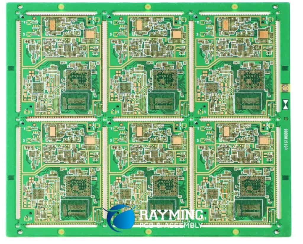
Panelization refers to the process of arranging multiple PCB layouts onto large panel sheets that serve as the base material. By grouping boards together on panels, improved efficiency and productivity can be achieved during the various fabrication steps.
In this comprehensive guide, we will explore the following topics around panelization:
Overview of Panelization
Panelization allows batch processing of PCBs by migrating multiple boards onto larger panels that take advantage of the full manufacturing line capacity. Groups of identical or different boards are arranged efficiently to use panel space.
The assembly panel serves as the transport mechanism through lamination, drilling, routing, testing, and other fabrication steps. Rather than processing single small boards, working with larger panels improves productivity.
Ultimately panels undergo depanelization with the individual PCBs separated through routing, breakaway tab or special fixture tools. The routed boards then proceed to component assembly and test.
Reasons for Panelization
There are compelling benefits panelization aims to achieve by collective PCB fabrication:
Cost Savings
Economies of scale by manufacturing panels containing multiples copies of a board is the driving incentive for panelization. By sharing common processes on panels, costs reduce proportionally to the increased number of boards.
Materials purchasing, fabrication setup charges, machine programming expenses amortize better across panels. Tight spacing efficiency allows maximizing these savings.
Assembly Process Optimization
Running panels through production instead of individual PCBs achieves:
- Streamlined workflow with fewer total units
- Sequential processing steps done in batches
- Balanced line loading and throughput
- Reduced handling minimizing misprocessing
These translate to tremendous throughput gains, faster turnaround and lower operational overheads.
Here is a summary view:
| Driver | Panelization Benefit |
|---|---|
| Cost | Bulk processing discounts |
| Efficiency | Higher throughput, less handling |
| Quality | Consistent processing |
Well-designed panel layouts are critical to leverage these benefits allowing panelized PCB production.
Panel Design Considerations
Several factors go into planning how boards layout on panels and organizing the panels themselves.
Panel Sizes
Standard PCB panel sizes derive from the substrate materials manufactured. Common panel dimensions include:
- 18” x 24”
- 21” x 24”
- 24″ x 18”
- 24” x 36″
Figure 1. Typical panel sizes
Fabricators stock these standard panel sizes so designs should conform for best cost savings. Custom or non-standard sizes sometimes apply but reduce batch efficiency.
Layout Arrangement
Panel space optimization happens in the PCB layout stage. Similar sized boards tile together on the panel with consistent spacing between copies. Boards orient optimally to minimize unusable space and waste.
High volume production runs replicate panels containing identical boards while prototypes may batch different boards to share test costs. Step stencil, routing path, lamination, drill stacks arrange compatible boards when mixing on common panels.
Designers arrange panels for:
- Efficient material utilization
- Balanced equipment processing loads
- Streamlined fabrication work flow
- Panel integrity under stresses
Tooling Rails and Fixtures
Tooling rails help hold boards in place and navigate the panel through fabrication. These additionally strengthen the panel periphery along with tab routings and outer breakaways. Rails fixture to jigs that prevent shifting of boards during conveyance through equipment.
Fiducials and markings aid alignment across processes like lamination layers stacking, drilling for holes alignment, automated optical inspection (AOI), testing points positioning.
Panelization Process Flow
Panelization occurs early once engineering layout completes. Main shared processing steps include:
1. Arrange designs: Engineers tile boards across panels ensuring spacing, symmetry constraints. Panel drawing files generate.
2. Fabricate panel: Batch panel processing performs artwork imaging, lamination, drilling, routing, plating, solder mask steps.
3. Test: Panels run comprehensive tests including bareboard insulation testing, opens/shorts checking, flying probe measurements.
4. Route/Breakapart: V-score routing and breakaway tab features assist separating boards from panels. Stress relief ensures no damage. Custom fixtured boards may directly proceed after this depanelization step.
5. Additional Assembly/Test: Further component assembly, inspection, functional testing completes the boards from the panels.
This shared sequence through initial fabrication, test, then breakout allows cost and efficiency benefits.
Depanelization
Depanelization constitutes the process of physically separating individual PCBs from the larger panels after common processing completes. This step can happen:
- At the PCB fabricator to supply tested boards ready for component assembly.
- At the contract manufacturer when board assembly commences.
Main depanelization techniques involve:
Routing/Scoring: V-shaped grooves score along board borders with a few connecting tabs. Operators snap boards apart manually or use fixtures for forceful separation.
Specialty Fixtures: Pogo-pins, gripping, or twisting fixtures mounted on panels align with tooling holes or edges to tear boards apart.
Breakaway Tab Routing: Paper-thin connections tab routed on panel borders that serve as frangible break points when shearing boards.
Depanelization applies stress so boards still attached to panels require careful handling to prevent cracking or delaminating. Completed boards get inspected after breaking away components or fixing hardware.
Design Guidelines for Panelization
Certain guidelines help engineers design boards keeping panelization in mind:
- Standard panel sizes maximize efficiency
- Include tooling holes with index markings
- Provision breakaway tabs on board outlines
- Define minimum spacing between boards
- Check lamination stresses don’t warp panels
- Enable stacking order and drill compatibility
- Allow identical processing steps when combining boards
Simplicity, reliability and consistency in the panel generation process allows smoother fabrication handling.
Panelization Design Rule Checking
While planning panels, running design rule checks helps avoid problems like:
- Inadequate spacing: ~0.2” spacing from tooling rails
- Insufficient tabs numbers: ~5 tabs for small boards
- Tab widths within safe range: 0.05” to 0.2″
- Missing fiducials for alignment
- Board warpage or panel breakage
Manual inspection or automated checks versus specified rules prevent costly revision.
Especially important is modeling lamination press stresses to ensure no panel bowing or breakage over temperature ramps. Pre-distortion programs may alter images to compensate for predictable material expansions.
Conclusion
Panelization enables optimized efficiency and cost savings in printed circuit board manufacturing by batch processing groups of boards together.
Careful panel design arranging boards, definining spacing constraints, tooling rails and other considerations help maximize fabrication line utilization while ensuring panel integrity.
By following panelization guidelines and design rule checks, engineers can build reliability into the resulting panel manufacturing constructs that handle boards collectively through production. Depanelization ultimates separates boards with close attention against inducing damage.
Well executed panelization unlocks order of magnitude productivity improvements during printed circuit board production runs, making the approach a ubiquitous mainstay of the industry.
Frequently Asked Questions
How does panelization provide cost savings for PCB production?
By processing batches of boards together on common panels, costs like materials purchasing, machine setup charges, tooling expenses amortize across larger volumes resulting in cost savings from economies of scale.
What are considerations when placing different PCB designs onto a single panel?
Key considerations when merging different boards onto common panels include:
- Compatible lamination layer count
- Same fabrication processing steps
- Shared drill bit sizes support
- Ensuring sufficient spacing and symmetry
Matching critical aspects allows panel fabrication without issues.
What are recommended minimum spacing values between boards on a panel?
Typical spacing rules for boards on panels are:
- 0.2 inch spacing from tooling rails
- 0.1 inch spacing around approval/registry stamp regions
- 0.05 inch general spacing between boards
Density maximizes while maintaining sufficient tolerance margins.
What are the main advantages of depanelization before PCB assembly?
Depanelizing before assembly allows factory automation to handle consistent sized individual boards with less indexing complexities. Separated boards also fit standard component insertion machines better with less guard rails interfering compared to irregular panel shapes.
How can stresses during PCB panel lamination be checked?
Static structural simulations of the full panel over expected temperature and humidity ranges during lamination curing is used to check any warpage or interlayer seperations. Pre-distortion of imaging may be used to compensate anticipating the material expansions.


0 Comments