
Pay Attention to Single Layer PCB Production
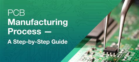
What is a Single Layer PCB?
A single layer PCB, also known as a single-sided PCB, is a printed circuit board that has conductive copper traces on only one side of the insulating substrate. The other side of the substrate is typically left bare or coated with a solder mask to protect the board from oxidation and improve its appearance.
Single layer PCBs are commonly used in simple electronic devices, such as:
- Radio frequency identification (RFID) tags
- LED lighting circuits
- Simple sensors and detectors
- Low-power amplifiers
- Basic power supply circuits
Advantages of Single Layer PCBs
Single layer PCBs offer several advantages over more complex multi-layer PCBs:
-
Cost-effectiveness: Single layer PCBs are generally less expensive to manufacture due to their simpler design and fewer materials required.
-
Faster production: The manufacturing process for single layer PCBs is typically quicker, as there are fewer steps involved compared to multi-layer PCBs.
-
Easier to design: Designing single layer PCBs is often more straightforward, as there are fewer considerations for layer stackup and interconnections.
-
Improved reliability: With fewer layers and connections, single layer PCBs are less prone to manufacturing defects and can be more reliable in certain applications.

Single Layer PCB Manufacturing Process
The manufacturing process for single layer PCBs involves several key steps:
-
PCB Design and Layout: The first step is to create the PCB design using specialized software, such as Altium Designer, Eagle, or KiCad. The design includes the component placement, copper trace routing, and any necessary annotations.
-
Substrate Preparation: The insulating substrate, typically made from materials like FR-4 or CEM-1, is cut to the desired size and shape. Holes for through-hole components are drilled, and the substrate surface is cleaned to ensure proper adhesion of the copper layer.
-
Copper Lamination: A thin layer of copper foil is laminated onto the prepared substrate using heat and pressure. The copper foil is typically pre-coated with a photoresist material.
-
Photoresist Exposure: The PCB design is transferred onto the photoresist-coated copper layer using a photolithography process. The photoresist is exposed to UV light through a photomask, which hardens the exposed areas while leaving the unexposed areas soluble.
-
Etching: The unexposed photoresist is removed using a chemical developer, exposing the unwanted copper areas. The board is then placed in an etching solution, typically ferric chloride or ammonium persulfate, which removes the exposed copper, leaving only the desired copper traces.
-
Solder Mask Application (optional): A solder mask layer can be applied to the PCB to protect the copper traces from oxidation and prevent solder bridges during the soldering process. The solder mask is typically applied using a silkscreen printing process and then cured using UV light.
-
Silkscreen Printing (optional): Labels, logos, and other markings can be added to the PCB using silkscreen printing. This process involves applying ink through a fine mesh screen onto the PCB surface.
-
Surface Finish (optional): A surface finish, such as HASL (Hot Air Solder Leveling), ENIG (Electroless Nickel Immersion Gold), or OSP (Organic Solderability Preservative), can be applied to the exposed copper areas to improve solderability and protect the copper from oxidation.
-
Quality Control and Testing: The manufactured PCBs undergo rigorous quality control checks and electrical testing to ensure they meet the required specifications and functionality.

Factors Affecting Single Layer PCB Production
Several factors can impact the quality and efficiency of single layer PCB production:
1. Material Selection
Choosing the right materials for your single layer PCB is crucial for ensuring optimal performance and reliability. The most common substrate materials for single layer PCBs are:
-
FR-4: A glass-reinforced epoxy laminate that offers good mechanical and electrical properties, as well as excellent heat resistance. FR-4 is the most widely used substrate material for PCBs.
-
CEM-1: A composite epoxy material that combines woven glass fabric and paper reinforcement. CEM-1 is less expensive than FR-4 but has lower mechanical and thermal properties.
-
Aluminum: Used in specific applications that require excellent heat dissipation, such as high-power LED lighting or motor control circuits.
The choice of copper foil thickness is also important, as it affects the current-carrying capacity and the ability to etch fine traces. Common copper foil thicknesses for single layer PCBs range from 0.5 oz to 2.0 oz per square foot.
2. Design Considerations
Proper PCB design is essential for ensuring manufacturability, reliability, and optimal performance. Some key design considerations for single layer PCBs include:
-
Trace width and spacing: Ensure that the copper traces are wide enough to carry the required current and are spaced adequately to prevent short circuits and signal interference.
-
Component placement: Place components in a logical and efficient manner to minimize trace lengths and improve signal integrity.
-
Soldermask and silkscreen: Use soldermask to protect the copper traces and prevent solder bridges. Silkscreen markings can improve assembly accuracy and provide useful information for maintenance and troubleshooting.
-
Design for manufacturing (DFM): Follow DFM guidelines to ensure that your PCB design is compatible with the manufacturing process and to minimize the risk of defects and delays.
3. Manufacturing Process Control
Maintaining strict control over the manufacturing process is essential for producing high-quality single layer PCBs consistently. Some key process control considerations include:
-
Etching process: Monitor and control the etching process parameters, such as solution concentration, temperature, and agitation, to ensure consistent and accurate copper removal.
-
Lamination process: Ensure that the lamination process achieves proper adhesion between the copper foil and the substrate, without causing defects like delamination or blistering.
-
Soldermask and silkscreen application: Control the thickness and coverage of the soldermask and silkscreen layers to ensure optimal protection and legibility.
-
Quality control and testing: Implement robust quality control procedures and testing protocols to identify and address any issues promptly.
4. Cost Optimization
Optimizing the cost of single layer PCB production is essential for maintaining competitiveness and profitability. Some strategies for cost optimization include:
-
Panelization: Group multiple PCB designs onto a single panel to maximize material utilization and reduce processing time.
-
Material selection: Choose cost-effective materials that meet the performance requirements of your application.
-
Design optimization: Simplify your PCB design to reduce the number of components, minimize trace lengths, and improve manufacturability.
-
Vendor selection: Partner with reliable and cost-competitive PCB manufacturers that can provide high-quality boards at competitive prices.

Single Layer PCB Production Challenges and Solutions
Despite the relative simplicity of single layer PCBs, manufacturers may face various challenges during production. Some common challenges and their solutions include:
1. Copper Trace Overetching
Challenge: Overetching occurs when the etching process removes too much copper, resulting in traces that are narrower than intended or even completely disconnected.
Solution: Monitor and control the etching process parameters closely, and consider using a more precise etching method, such as spray etching or laser direct imaging (LDI).
2. Soldermask Adhesion Issues
Challenge: Poor soldermask adhesion can lead to peeling, chipping, or bubbling of the soldermask layer, exposing the copper traces to oxidation and potential damage.
Solution: Ensure that the PCB surface is properly cleaned and prepared before applying the soldermask. Use high-quality soldermask materials and follow the manufacturer’s application guidelines closely.
3. Silkscreen Legibility
Challenge: Poorly applied or low-quality silkscreen markings can be difficult to read, leading to assembly errors and difficulties in maintenance and troubleshooting.
Solution: Use high-quality silkscreen inks and screens, and ensure that the silkscreen artwork is properly designed and aligned. Consider using alternative marking methods, such as direct legend printing or laser marking, for improved legibility and durability.
4. Copper Thickness Variations
Challenge: Inconsistent copper thickness across the PCB can lead to performance issues and reduced reliability, particularly in high-current applications.
Solution: Use high-quality copper foils with consistent thickness, and monitor the lamination process to ensure even pressure and temperature distribution. Consider using alternative copper deposition methods, such as electroplating, for improved thickness control.
Single Layer PCB Production Best Practices
To optimize your single layer PCB production process and ensure high-quality, reliable boards, consider implementing the following best practices:
-
Collaborate closely with your PCB design team: Foster open communication between the design and manufacturing teams to ensure that the PCB design is optimized for manufacturability and performance.
-
Invest in quality materials: Choose high-quality substrates, copper foils, and soldermask materials to minimize the risk of defects and ensure optimal performance.
-
Implement a rigorous quality control process: Establish comprehensive quality control procedures and testing protocols to identify and address any issues promptly.
-
Monitor and optimize process parameters: Regularly monitor and fine-tune the manufacturing process parameters, such as etching, lamination, and soldermask application, to ensure consistent and high-quality results.
-
Stay up-to-date with industry trends and technologies: Keep abreast of the latest developments in PCB manufacturing, such as new materials, processes, and equipment, and evaluate their potential benefits for your production process.
Single Layer PCB Production FAQ
-
Q: What is the typical turnaround time for single layer PCB production?
A: The turnaround time for single layer PCB production varies depending on the complexity of the design, the quantity ordered, and the manufacturer’s capacity. Typically, small to medium-sized orders can be completed within 1-2 weeks, while larger or more complex orders may take 3-4 weeks or longer. -
Q: Can single layer PCBs be used for high-frequency applications?
A: Single layer PCBs can be used for some high-frequency applications, such as simple RF circuits or antenna designs. However, for more complex high-frequency applications, multi-layer PCBs with controlled impedance and shielding may be necessary to ensure optimal signal integrity and minimize interference. -
Q: Are single layer PCBs suitable for automated assembly?
A: Yes, single layer PCBs can be designed for automated assembly by following design for manufacturing (DFM) guidelines, such as providing adequate component spacing, using standard component sizes, and avoiding excessively small or narrow features. -
Q: Can single layer PCBs be manufactured with different surface finishes?
A: Yes, single layer PCBs can be manufactured with various surface finishes, such as HASL (Hot Air Solder Leveling), ENIG (Electroless Nickel Immersion Gold), or OSP (Organic Solderability Preservative), depending on the application requirements and the manufacturer’s capabilities. -
Q: How can I ensure the reliability and longevity of my single layer PCBs?
A: To ensure the reliability and longevity of your single layer PCBs, consider the following: - Use high-quality materials and components
- Follow best practices for PCB design and manufacturing
- Implement a robust quality control process
- Protect the PCB from environmental factors, such as moisture, dust, and extreme temperatures
- Perform regular maintenance and inspections to identify and address any issues promptly
Conclusion
Single layer PCB production is a crucial aspect of electronic device manufacturing, and understanding the key factors that influence the production process is essential for ensuring high-quality, reliable, and cost-effective PCBs. By considering the material selection, design considerations, manufacturing process control, and cost optimization strategies discussed in this article, you can optimize your single layer PCB production process and stay competitive in today’s rapidly evolving electronics industry.
As technology advances and new applications emerge, staying up-to-date with the latest trends and best practices in single layer PCB production will be crucial for success. By fostering collaboration between design and manufacturing teams, investing in quality materials and processes, and continuously improving your production workflow, you can position your organization to meet the challenges and opportunities of the future.
| Single Layer PCB Production | Key Considerations |
|---|---|
| Material Selection | FR-4, CEM-1, Aluminum, Copper Foil Thickness |
| Design Considerations | Trace Width & Spacing, Component Placement, Soldermask & Silkscreen, DFM |
| Manufacturing Process Control | Etching, Lamination, Soldermask & Silkscreen Application, Quality Control & Testing |
| Cost Optimization | Panelization, Material Selection, Design Optimization, Vendor Selection |
Table 1: Key considerations for single layer PCB production.
By focusing on these key aspects of single layer PCB production and implementing the best practices and solutions discussed in this article, you can ensure that your PCBs meet the highest standards of quality, reliability, and performance, while also optimizing costs and efficiency. With a solid understanding of single layer PCB production, you can position your organization for success in the dynamic and competitive world of electronic device manufacturing.