Introduction
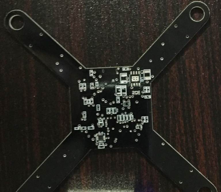
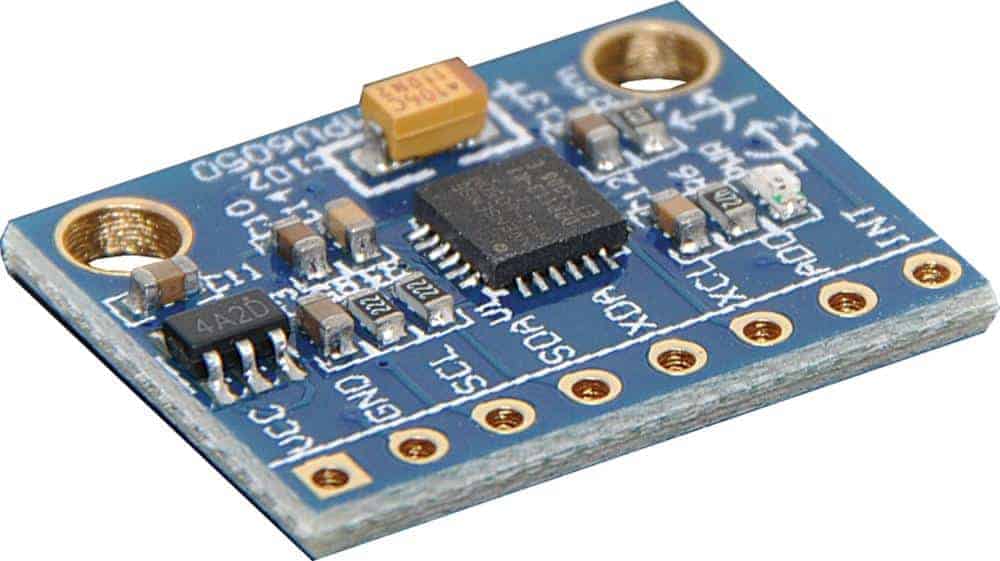
Printed circuit boards (PCBs) are essential components in most modern electronic devices. They provide the physical platform to mount and connect electronic components using conductive copper traces etched from copper sheets laminated onto a non-conductive substrate. PCBs allow electronic circuits to be compactly assembled in a rugged package.
The process of taking an electronic circuit idea and turning it into a physical PCB involves several steps:
- Schematic design
- PCB layout
- Component selection
- PCB fabrication
- PCB assembly
- Testing
In this guide, we will explore the key concepts and steps involved in PCB design and assembly.
Schematic Design
The first step is creating the circuit schematic. This is a visual diagram showing the logical connections between electronic components and often drawn using CAD software. The schematic depicts components as symbols and their interconnections through wires.
Schematics should adhere to design principles like:
- Clear visual presentation
- Logical grouping of related components
- Minimal crossing of wires
- Hierarchical organization using sheets
- Complete component information
- Annotation such as reference designators
CAD tools allow simulation of the circuit schematic to verify its electrical performance before physical implementation as a PCB.
PCB Layout
With the schematic completed, the PCB layout can be started. This involves specifying the physical footprint of components and routing connections on board layers.
Key factors in PCB layout:
Component Footprints
The physical dimensions and pad shapes for soldering each component become its footprint on the PCB. Standard footprints are available in CAD libraries. Custom footprints may need to be created for specialized components.
Placement
Components need to be intelligently placed on the PCB considering factors like:
- Circuit topology and net connections
- High density placement
- Thermal considerations
- Access for debugging, testing, and servicing
Routing
Routing creates copper traces to connect component footprints according to the schematic netlist. This must balance length matching, impedance control, noise reduction, and high-density routing.
Key guidelines for routing are:
- Minimize trace lengths
- Use appropriate trace widths for current
- Match lengths of critical nets
- Use 45/90 degree angles
- Avoid routing between dense component placements
PCB Stackup

Another vital PCB layout consideration is stackup – the layer structure of the PCB. A minimum 2-layer board has copper on top and bottom. Additional inner layers can be added for complex, high-density boards.
Key considerations for stackup design:
- Number of routing layers required
- Signal layer positioning – next to plane layer for shielding
- Plane layer purposes – power, ground, shielding
- Layer thickness – thinner dielectric improves impedance control
- High-speed materials – FR4, Rogers, polyimide
- Different dielectrics can be combined
- Impedance control based on trace geometry
Component Selection
The schematic depicts generic components. These now need to be mapped to real-world parts for the PCB. Components are selected considering factors like:
- Functionality – logic devices, microcontrollers, analog parts
- Performance – speed, power, accuracy, tolerance
- Cost – pricing, availability
- Physical parameters – package, footprint, height
- Reliability – environment, lifespan, quality
Preferred parts that are standard to the company or industry should be used where possible. Critical components may need additional sourcing.
PCB Fabrication
Once the PCB layout is finalized, production files are sent for board fabrication. Key steps are:
Output Generation
The CAD tool outputs Gerber files and drill files for board fabrication. Excellon or Sieb & Meyer are common drill file formats.
Panelization
To optimize production, PCBs are arranged on larger panels that are batch fabricated together. Software allows automated panelization.
Cam Processing
The PCB manufacturer processes the Gerber and drill files through CAM software to setup fabrication. This validates the design and extracts manufacturing data.
Lamination
Sheets of copper-clad laminate are stacked up to form a multilayer board. The layers are aligned and laminated under heat and pressure.
Drilling
Holes are drilled through the laminated stack to form vias for vertical interconnections between layers. Excellon NC drill files guide hole positions and sizes.
Etching
Unwanted copper is etched away to leave only the desired conductive traces on each layer, revealing the PCB circuit pattern.
Plating and Coating
Surfaces are plated with solder or gold. Protective silkscreen and solder mask coatings are applied. Holes may be plated for conductivity.
Scoring and Depaneling
Finished boards are scored and routed to separate individual PCBs from panels. They are then sent for assembly.
PCB Assembly

Populating a bare PCB with components is called assembly or PCA (Printed Circuit Assembly). This typically involves:
Solder Paste Application
Solder paste is screen printed or dispensed on PCB pads. This provides adhesive for component placement and soldering.
Pick and Place
Robots precisely pick components and place them onto the solder paste footprints on the board. Accuracy of a few microns is achievable.
Reflow Soldering
The populated board passes through a reflow oven. The solder paste melts, fusing components to pads.
Conformal Coating
A protective coating may be applied over the assembled board, leaving connectors exposed.
Programming/Testing
For boards with firmware, this is loaded. Testing and inspection verifies assembly quality.
PCB assembly can be done in high volumes using SMT lines. For prototypes and small batches, hand assembly or semi-automated assembly may be suitable.
Design for Manufacturing and Assembly
PCBs designed effectively for manufacturing and assembly achieve higher yield, quality, and reliability. Some guidelines:
- Allow adequate spacing between components and traces
- Use standard pad shapes/sizes for ease of soldering
- Avoid tiny or dense parts in inner layers
- Follow assembly process rules like solder mask defined pads
- Facilitate test probe access
- Include testpoints, fiducials, and adequate markings
- Use entry-level friendly connectors
- Select PCB finish suitable for assembly process
Testing PCBs
Testing validates the quality and correct function of the assembled PCB. It involves:
In-Circuit Testing – electrical testing of populated boards for shorts, opens, correct resistance.
Functional Testing – exercising the inputs/outputs and operating the board to verify performance.
Burn-in Testing – environmental stress testing under temperature, vibration to weed out early failures
Automated Optical Inspection – camera imaging to check assembly defects and solder joint quality.
Testing should cover key parameters specific to the product – logic, analog performance, interfaces, etc. Test coverage and diagnostics capabilities are important for smooth manufacturing.
Conclusion
In summary, PCB design and assembly incorporates schematic capture, layout, fabrication, component assembly, and testing to transform an electronic circuit concept into a physical working product. Adhering to sound design practices across the process enables building high quality boards in a cost-effective manner. With the growth in electronics across industries, PCB technology will continue to enable innovative devices and solutions.
Frequently Asked Questions
What are some key factors to consider during PCB layout?
Some key factors are: component placement for optimal routing, minimizing trace lengths, matching net lengths, routing at 45/90 degrees, choosing layer stackup, and allowing sufficient spacing between traces and pads.
How is impedance controlled in PCBs?
Impedance is controlled through trace width/thickness and proximity to the reference plane. Thinner dielectrics help improve impedance control. High-speed materials like FR4, Rogers, Polyimide also have consistent dielectric properties.
What panelization approaches are used in PCB fabrication?
Common panelization techniques are X-axis or Y-axis scoring/routing, tab routing (V-scoring), and tooling holes with tooling strips. This arranges arrayed boards for batch processing and separation after fabrication.
What types of automated soldering are used for PCB assembly?
Typical automated soldering processes are reflow soldering in a convection oven and selective wave soldering. Reflow works for SMT components, while wave soldering can solder through-hole parts. Some boards use a combination.
Why is testing important in PCB manufacturing?
Testing is critical to ensure consistent quality. It verifies there are no assembly defects or functional issues with the populated boards. This helps catch problems early and prevent costly field failures.


0 Comments