Introduction
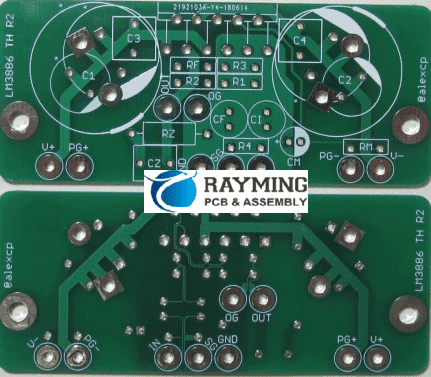
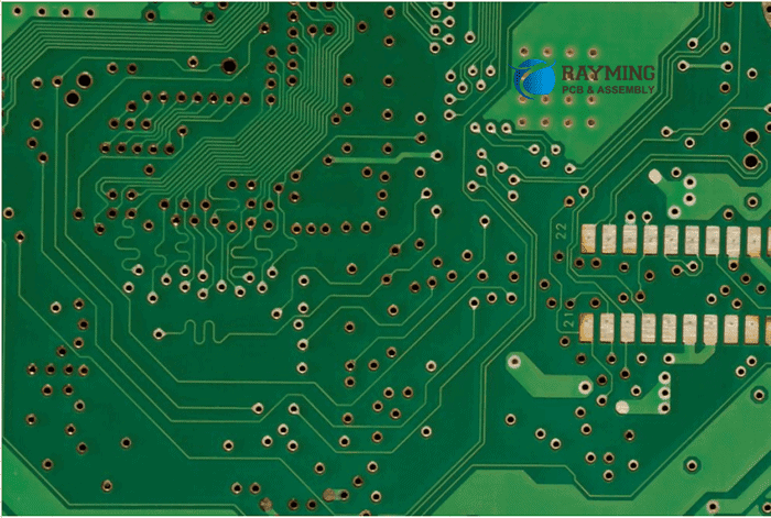
Printed circuit boards (PCBs) provide the foundation for electronics products and equipment. PCB assembly is the process of soldering or otherwise attaching electrical components to the PCB to create a functional printed circuit assembly (PCA). The PCB design, components used, and assembly process all contribute to determining the performance and reliability of the final PCA.
This guide provides a comprehensive overview of PCB assembly. It covers:
- PCB assembly process steps
- Surface mount vs through-hole components
- Soldering techniques
- Cleaning and inspection
- Testing assembled boards
- Quality control
- Assembly challenges
- Process documentation
- Outsourcing vs in-house assembly
- Cost tradeoffs
Understanding the key factors in PCB assembly helps ensure robust, high-quality boards that meet requirements.
PCB Assembly Process Overview
The assembly process involves mounting and soldering components onto a fabricated PCB. Here are the typical steps:
- PCB fabrication – The bare PCB is fabricated based on your design files.
- Stencil creation – A metal stencil is laser cut with solder paste openings matching the PCB footprint.
- Solder paste application – Solder paste is screen printed or dispensed through the stencil.
- Component placement – Parts are accurately placed on solder paste deposits.
- Soldering – The board passes through a reflow oven melting the solder to attach components.
- Cleaning – Flux residue is cleaned from the assembled board.
- Inspection – Boards, solder joints and component placement are inspected.
- Testing – Electrical tests validate assembly and board functionality.
- Conformal coating – A protective coating may be applied.
- Final inspection – Board appearance, dimensions, and markings are checked before shipment.
Each step must be done properly to reliably assemble PCBs.

Surface Mount and Through-Hole Component Differences
Two main technologies are used to mount components onto PCBs:
Surface mount – Parts have metal pads that solder directly to the surface of the PCB. Smaller size and faster automated assembly.
Through-hole – Leads pass through holes in the PCB and are soldered on the opposite side. Larger but simpler manual assembly.
| Parameter | Surface Mount | Through-Hole |
|---|---|---|
| Part Size | Smaller | Larger |
| Height | Low profile | Stand off board farther |
| Assembly Method | Automated | Manual |
| Assembly Speed | Faster | Slower |
| Cost | Lower | Higher |
| Automated Testability | Better | Worse |
| Reworkability | Harder | Easier |
For automated assembly of higher density boards, surface mount dominates today. But through-hole still suits some large components or harsh environments.
Soldering Processes for PCB Assembly
Soldering electrically and mechanically attaches components to PCBs. The main techniques are:
- Reflow soldering – For surface mount parts. Solder paste is reflowed in an oven.
- Wave soldering – For through-hole parts. PCB bottom passes over molten wave.
- Hand soldering – Manual soldering for rework or holes.
- Selective soldering – Automated soldering of through-hole connectors.
- Vapor phase soldering – Condensing vapor used for temperature stability.
The right soldering process depends on factors like:
- Part sizes and types
- Production volume
- Desired process quality
- Equipment costs targeted
Reflow soldering handles the majority of PCB assembly volume today. But many boards use a combination of soldering techniques.
Cleaning Assembled Boards
Solder flux residues left on the PCB must be cleaned to prevent corrosion or electrical issues. Cleaning methods:
- Aqueous cleaning – Detergent solution to wash boards.
- Solvent cleaning – Strong solvents break down and remove residues.
- Plasma cleaning – Plasma energy dissolves residues.
- Laser ablation – Pulsed laser blasts vaporize residues.
Thorough cleaning is essential after soldering. In consumer electronics, no-clean flux has become popular to eliminate this step. But aerospace and military applications still require meticulous cleaning.
Inspecting Assembled PCBs
Multiple inspection stages ensure assembly quality:
| Inspection Phase | Typical Methods | Defects Detected |
|---|---|---|
| Solder Paste Inspection | Stencil microscope, SPI | Insufficient paste deposits |
| Post Placement | Automated optical inspection (AOI) | Misalignments, missing parts |
| Post Reflow | AOI, X-ray, Solder joint inspector | Solder defects, tombstoning |
| Final inspection | AOI, optical microscope | Marking defects, cosmetic issues |
Advanced automated optical inspection systems can identify tiny soldering defects and component problems. This improves quality and prevents rework.
Testing PCB Assemblies
Testing verifies board assembly and functionality:
- In-circuit test (ICT) – Tests electrical connectivity and functions between components. Catches assembly defects.
- Flying probe – Tests connectivity of pads/traces. Checks for shorts and opens.
- Boundary scan – Tests at component boundaries using scan chains. Needs support built-in.
- Functional test – Validates entire board functions properly as a system. Confirms performance.
| Test Type | Coverage | Speed | When Used |
|---|---|---|---|
| In-circuit | High | Moderate | After assembly |
| Flying probe | Moderate | Fast | During prototyping |
| Boundary scan | High | Slow | Complex boards |
| Functional | Complete | Slow | End of line |
Adding testing does increase assembly costs. But it improves quality and reliability for more complex or mission-critical boards.

Quality Control in PCB Assembly
Maintaining quality control throughout the assembly process is vital:
- Component management – Ensure proper storage, handling, inspection of parts.
- Process control – Validate process parameters stay within specification.
- Equipment maintenance – Prevent variation through scheduled maintenance and calibration.
- ESD control – Follow anti-static procedures when handling boards and components.
- Inspection and testing – Find any defects and prevent shipment of bad boards.
- Personnel training – Educate team on proper assembly methods to avoid human errors.
- Data analysis – Apply statistical process control to identify process improvement opportunities.
A focus on quality and continuous improvement reduces defects and avoids costly rework.
Common PCB Assembly Challenges
Engineers must anticipate and address potential assembly challenges:
- Solder bridges – Unwanted solder connections shorting traces. Careful soldering process controls required.
- Solder balls – Spheres of solder creating shorts. Usually from solder paste handling issues.
- Tombstoning – Part tilts upright from one pad lifting during reflow. Indicator of process issues.
- Voids – Bubbles trapped in solder joint, potentially reducing strength. Cause may be paste quality, part position, heating.
- Warping/twisting – Board warpage from uneven heating. Can impair soldering results.
- ESD damage – Static discharge can destroy sensitive components. Needs proper grounding, ionization, handling.
- Contamination – Particles or residue preventing effective soldering. Clean processes are essential.
With experience and vigilance, these common defects can be minimized or eliminated.
Process Documentation
Documenting assembly procedures and acceptance criteria is essential:
- Assembly drawings – Illustrate component placement, orientations, markings.
- Work instructions – Detailed steps for each process operation.
- Acceptance standards – Criteria for passing inspection and testing.
- Training records – Document training of assembly personnel.
- Process data – Record process parameters and results to analyze trends.
Thorough documentation enables assembly repeatability and aids root cause analysis when defects occur.
In-House Assembly vs Outsourcing
Companies must decide whether to assemble PCBs in-house or outsource:
In-house
- More control over quality and IP
- Faster turnaround on design changes
- Lower volumes more economical
Outsourcing
- Leverages assembly expertise and facilities
- Handling of higher volumes more cost effective
- Equipment costs avoided
In general, outsourcing is better for higher volume production. For advanced processes, unique requirements, and quick-turn prototyping, in-house assembly may be preferred.
PCB Assembly Cost Considerations
The costs of PCB assembly include:
- Labor – Manual assembly steps require operator time and expertise.
- Equipment – Soldering machines, inspection systems, and facility overhead.
- Components – BOM parts costs, including small passives, connectors, ICs.
- Testing – Added verification steps and handling to test boards.
- Rework – Labor and materials to correct defective boards.
Ways to potentially lower assembly costs:
- Simplify board and part designs
- Eliminate through-hole parts
- Reduce layer counts
- Increase production volumes
- Specify common components
- Control soldering process tightly
- Reduce testing
Assessing PCB assembly costs during design allows tradeoffs between upfront and back-end economics.
Conclusion
PCB assembly transforms bare circuit boards into functioning electronic systems. The processes must be controlled to avoid defects and meet quality and reliability requirements. Understanding the steps for assembly, inspection and test enables manufacturing robust, high-performance PCBs. By planning for assembly, maximizing process capability, and verifying quality, companies can ship boards that successfully meet their product needs.
FAQ
What are some key factors impacting PCB assembly costs?
Major cost drivers are board complexity, layer count, component types, soldering process difficulty, testing needs, production volumes, rework rates, and manufacturing location. Simpler boards in higher volumes generally cost less.
What defects should be inspected for after soldering PCB assemblies?
Critical post-solder inspection checks for solder bridges, solder voids, poor wetting, missing/misaligned parts, lifted pads, and damage from heat or handling. Automated optical inspection provides thorough examination.
How small of components can be reliably surface mounted on a PCB?
With advanced soldering, inspection, and handling processes, surface mount parts can be as small as 01005 size (0.4mm x 0.2mm). Skilled operators and microscopes aid manual handling of tiny SMT parts.
What are considerations when outsourcing versus assembling PCBs in-house?
In-house assembly allows more process control and IP protection but requires equipment and staff. Outsourced assembly leverages vendor expertise and facilities but reduces hands-on quality control. Volumes and complexity factor into the decision.
What can I do to improve soldering quality and prevent defects on our PCB assemblies?
Maintaining tight process controls, operator training, inspection at each step, scheduled machine maintenance, analyzing defects root causes, and implementing process improvements are key to maximizing soldering quality.


0 Comments