Introduction to PCBA Manufacturing
Printed circuit board assembly (PCBA) manufacturing is the process of soldering electronic components to a printed circuit board (PCB). The assembled PCB, known as a PCBA, forms the backbone of all electronic devices. From simple devices like calculators to complex gadgets like smartphones and computers, every electronic product relies on PCBAs.
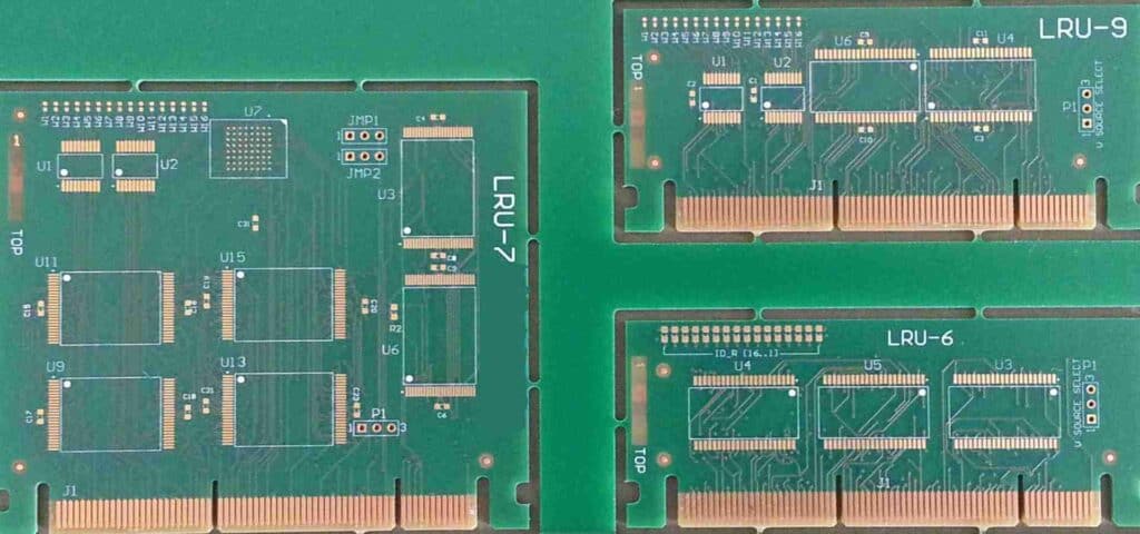
The PCBA manufacturing process involves soldering components like resistors, capacitors, integrated circuits (ICs), transistors, and other parts on to the PCB. PCBs provide the mechanical structure to mount components and connect them together through copper tracks etched on the board. PCBAs thus comprise a PCB populated with electronic components soldered on to it through metal tracks.
PCBA manufacturing typically involves the following key stages:
Stages of PCBA Manufacturing
- PCB Fabrication – Making bare PCBs by etching copper layers on an insulating substrate
- Stencil Printing – Applying solder paste on PCB pads for component placement
- Component Placement – Mounting components on their designated pads
- Reflow Soldering – Melting solder paste to form solder joints and affix components
- Testing and Inspection – Verifying electrical connectivity and functionality
- Conformal Coating – Applying protective coating on assembled PCBs
Why Outsource PCBA Manufacturing?
With the miniaturization of electronics and products becoming more compact, PCB designs have become extremely complex. Manufacturing such intricate PCBAs requires significant investments in facilities, equipment, and expertise. Most technology companies find it economical to outsource PCBA production to a specialist manufacturer. The key benefits of outsourced PCBA manufacturing include:
- Cost Savings – Eliminates investment in production infrastructure
- Specialization – Leverages expertise and experience of an Electronics Manufacturing Services (EMS) provider
- Quality – Assured quality as per IPC standards at accredited facilities
- Reliability – Access to advanced manufacturing and inspection technologies
- Flexibility – Scales production capacity as per demand fluctuations
- Reduced Time-to-Market – Faster turnaround through streamlined processes
- One-stop Shop – Value-added services including component sourcing, logistics
How to Select a PCBA Manufacturing Partner
Choosing the right EMS partner is crucial in ensuring quality, reliability, and cost-effectiveness of your PCBA production. Here are some key factors to consider when selecting a PCBA manufacturing provider:
Key Selection Criteria
| Factor | Description |
|---|---|
| Technical Capabilities | Sophisticated SMT lines, advanced test systems, expertise in PCBA technologies |
| Quality & Certifications | ISO 9001, IATF 16949, AS9100 certifications demonstrate capabilities |
| Industry Experience | Knowledge of the latest trends, technologies, and solutions in vertical markets |
| Volume Scalability | Ability to adjust production capacity flexibly as per changing demand |
| Lead Time & Turnarounds | Quicker turnaround times indicate streamlined processes |
| Pricing Structure | Competitive and transparent pricing models |
| Value-added Services | Design support, component sourcing, inventory management enhances convenience |
| Responsiveness | Quick response to RFQs, engineering changes, and production issues |
PCBA Manufacturing Process Step-by-Step
PCBA manufacturing involves intricately assembling thousands of tiny components on complex PCBs. Each step in the sequence needs careful control and inspection to build quality boards.
Here is a step-by-step breakdown of the PCBA manufacturing process:
1. Solder Paste Printing
Solder paste is first applied on the PCB pads where components need to be soldered. This is done precisely using stencils and solder paste printing equipment. The solder paste temporarily holds the components in place before soldering.
2. Component Placement
Electronic components are accurately positioned on their designated PCB pads according to the bill of materials (BOM). Pick and place machines place thousands of parts per hour on PCBs. For large components, manual placement may be needed.
3. Solder Reflow
The assembled PCBs pass through reflow ovens that melt the solder paste to form permanent solder joints. Different soldering techniques can be used depending on component types and PCB complexity.
4. Cleaning
Any post-soldering residue or flux is cleaned off the PCBs using suitable cleaning agents. Cleaning removes impurities and improves solder joint integrity.
5. Automated Optical Inspection
PCBAs are inspected under advanced optical systems to check for any missing, misaligned or improperly soldered components. Errors spotted are resolved before further production.
6. In-circuit Testing
Electrical tests validate connectivity between components, identify any shorts or opens, and verify board functionality. Faulty PCBAs can be reworked to fix issues.
7. Conformal Coating
A protective plastic coating is applied on assembled boards to shield against moisture, dust, chemicals and temperature damage during product use.
8. Final Testing
Finished PCBAs undergo comprehensive testing using test fixtures to validate complete functionality. Parameters like continuity, voltages, performance are evaluated.
9. Marking and Packaging
PCBAs are labeled for identification. They are packed into ESD-safe packaging to prevent electrostatic discharge damage during storage and transit.
Key PCBA Manufacturing Technologies
PCBA manufacturing utilizes a range of advanced technologies and equipment to enable sophisticated SMT production.
Surface Mount Technology (SMT)
SMT assembly attaches components directly onto the PCB surface rather than through holes. This enables miniaturized and high-density PCBAs ideal for small gadgets.
Solder Paste Printing
Automated stencil printers apply the right amount of solder paste accurately onto PCB pads for reliable component soldering.
Pick-and-Place Systems
High speed pick-and-place machines precisely position thousands of tiny SMT components per hour on PCBs. Advanced systems feature multiple heads and high accuracy.
Reflow Soldering
Different techniques like convection, vapor phase, and infrared reflow solder PCB assemblies by heating solder paste deposits. This bonds components to pads.
Automated Optical Inspection (AOI)
AOI systems use sophisticated cameras and software to inspect assembled PCBs for defects in real-time with high reliability.
In-Circuit Test (ICT) Systems
ICT fixtures electronically verify that PCB components and circuits are properly connected and functioning before the product is finished.
X-Ray Inspection
X-ray imaging validates solder joint quality and checks for issues like voids, bridging and missing connections under components.
Quality Control in PCBA Production
Maintaining quality across the many intricate production steps is critical in PCBA manufacturing. Some key quality assurance measures include:
- Statistical process control to prevent process variability
- Incoming quality control of components, solder paste, etc
- Automated optical inspection of assembled PCBs
- ICT testing to verify board assembly integrity
- Reliability testing like HAST, thermal cycling, vibration to validate robustness
- ESD control to prevent electrostatic discharge damage
- Traceability systems to track and isolate defects
- Documentation control using manufacturing data management systems
By following IPC standards and maximizing process automation, modern EMS providers achieve over 99% defect-free PCBA production.
PCBA Manufacturing Defects
Despite rigorous quality control, some defects may occur during PCBA production. Common PCBA defects include:
| Defect | Cause | Effect |
|---|---|---|
| Missing components | Pick-and-place error | Circuit malfunction |
| Wrong component | Incorrect setup/programming | Performance issues |
| Misaligned parts | Inaccurate placement | May cause short circuits |
| Tombstoning | Unbalanced solder paste deposition | Interconnection failure |
| Solder bridges | Excess solder buildup | Electrical shorts |
| Solder voids | Poor wetting, insufficient heat | Can impact reliability |
| Solder balls | Excess solder | Potential shorts |
| Cracked joints | Thermal/mechanical stress | May increase resistance |
Advanced inspection systems and testing methodologies help identify and address assembly issues before shipment.
Key Considerations in PCBA Design
PCB design considerations impact manufacturability, testability, and long-term reliability of the assembled board. Here are some key aspects designers should account for:
- Component Selection – Choose components compatible with assembly processes and board technology
- PCB Layout – Optimize layout for manufacturing and functionality
- SMT Design – Enable adequate spacing, pad sizes, etc. for SMT assembly
- BOM Optimization – Reduce component count and types to lower cost
- Design for Testability – Consider test points, fixtures, and interfaces
- Thermal Management – Ensure proper cooling for heat-emitting components
- Reliability Factors – Withstand vibration, shock, temperature, and other stresses
- RoHS Compliance – Select RoHS-compliant PCB and component finishes
Involving manufacturing engineers early in the design stage helps create optimal PCBA designs.
The Importance of PCBA Documentation
Maintaining proper documentation is vital for effective PCBA manufacturing. Key documents required include:
- Bill of Materials (BOM) – Details all components to be assembled on the PCB
- Assembly Drawings – Illustrates component placement, soldering profiles, board overlay
- Schematics – Shows electrical connectivity between parts
- Gerber Files – PCB layer images for fabrication
- PCB Footprint Drawings – Specifies pad dimensions for each component
- Assembly Instructions – Defines the step-by-step build sequence
- Test Specifications – Test parameters, procedures and pass/fail criteria
- Certificate of Conformance (CoC) – Declares that delivered PCBAs meet requirements
With comprehensive documentation, PCBA production and testing can be executed accurately as per specifications.
FAQs on PCBA Manufacturing
Q: What are the different PCBA testing methods?
A: Major PCBA testing techniques include visual inspection, in-circuit test (ICT), flying probe test, boundary scan, automated x-ray inspection (AXI), and functional testing. ICT and functional testing are most widely used to validate electrical performance and functionality.
Q: How are components affixed on double-sided or multi-layer PCBs?
A: Plated through-hole (PTH) technology creates interconnections between layers in multilayer boards. Components are soldered on the outer layers, while barrels go through holes to connect inner layers. Some components may use surface mount pads on outer layers along with PTH barrels.
Q: What materials are used to make PCBs?
A: The most common PCB substrate is FR-4 glass epoxy. This offers good strength, dielectric properties, heat resistance and cost-effectiveness. High frequency boards use advanced substrates like polyimide, PTFE, ceramic, etc. Copper makes up the conductive traces and pads.
Q: How can EMS providers manage fluctuating demand?
A: By forming supply chain partnerships and an extensive service provider network, EMS providers can scale production capacity flexibly to meet changing requirements. They leverage optimized inventory and production control systems.
Q: What is HAST testing?
A: Highly Accelerated Stress Test (HAST) accelerates the effects of temperature and humidity to validate product reliability. HAST exposes PCBAs to conditions like 100% humidity at 130°C for rapid aging. PCBAs passing HAST exhibit robust resistance to moisture and thermal stress during operation.


0 Comments