Introduction
Printed circuit boards (PCBs) are essential components in almost all electronic devices, from smartphones and computers to industrial equipment. A PCB provides the mechanical structure to mount and interconnect electronic components using conductive pathways or traces etched from copper sheets laminated onto a non-conductive substrate.
The PCB manufacturing and assembly process is complex, involving many steps to transform raw materials into a fully functioning board. This article will provide a comprehensive overview of PCB fabrication, covering everything from design and materials selection to manufacturing, assembly, and testing.
PCB Design and Materials
The first step in the PCB production process is designing the board layout. PCB design is generally done using CAD (computer-aided design) software like Altium, Cadence Allegro, and KiCad. The designer must consider the circuit requirements, number of layers, component placement, routing, and other factors.
Once the board layout is finalized, the next step is selecting the proper substrate and lamination materials. Important material properties like dielectric constant, thermal conductivity, CTE (coefficient of thermal expansion), and moisture absorption must be evaluated. Here are some of the most common materials used in PCB fabrication:
- Substrate – FR-4 (glass reinforced epoxy), polyimide, ceramic
- Copper foil – Rolled copper, electro-deposited copper
- Soldermask – Liquid photoimageable, dry film
- Silkscreen – Epoxy or acrylic-based ink
PCB Stackup
The PCB stackup refers to the layer structure of the circuit board. A simple 2-layer board consists of a single copper layer on the top and bottom of the substrate. Multilayer boards can have anywhere from 4 to 30+ layers stacked up, allowing complex circuit routing.
Here are some typical layer stackups:
- 2-layer: Copper-Substrate-Copper
- 4-layer: Copper-Substrate-Copper-Substrate-Copper
- 6-layer: Copper-Substrate-Copper-Substrate-Copper-Substrate-Copper
High layer count boards will often incorporate different material thicknesses and copper weights in the stackup for optimal electrical and thermal performance.
PCB Fabrication Process
The PCB fabrication process can be grouped into three main steps: imaging, etching, and lamination. Advanced PCB shops use sophisticated equipment to produce boards with extremely fine features and tight tolerances.
Imaging
The imaging process transfers the PCB design onto the copper clad substrate. There are two primary imaging methods:
- Photolithography – A photomask with the pattern is projected onto a photosensitive substrate using UV light. The exposed areas become soluble.
- Direct Imaging – A laser or ion beam directly writes the pattern onto the photoresist coating on the copper.
After imaging, the soluble photoresist is washed away, leaving a bare copper pattern.
Etching
Etching removes the unwanted copper, isolating the conductive traces. The two main etching techniques are:
- Wet Etching – The boards are immersed in an etchant chemical bath. Ferric chloride and ammonium persulfate are common etchants.
- Dry Etching – Plasma energy removes exposed copper by sputtering. Environmentally clean but slower.
Wet etching is faster and cheaper but requires disposal of hazardous chemicals. Dry etching is more precise.
Layer Lamination
Individual etched copper layers are stacked up and laminated together under heat and pressure. Prepreg sheets (fiberglass impregnated with resin) are interleaved between layers. Lamination fuses the layers into a single board.
Drilled holes called vias provide electrical connections between layers. Plated through-hole (PTH) vias are coated with copper electroplating.
Common PCB Types
There are several common types of PCBs, classified by the substrate material and number of layers:
- FR-4 Boards – Most common. FR-4 glass epoxy substrate. Low cost.
- Rigid Flex Boards – Combines rigid FR-4 with flexible polyimide substrates.
- Metal Core Boards – Insulated metal substrate for high thermal performance.
- Ceramic Boards – Alumina or aluminum nitride substrate. Costly but handles high frequency, temperature, and power.
- Flex Boards – Flexible polyimide substrate. Used in dynamic applications.
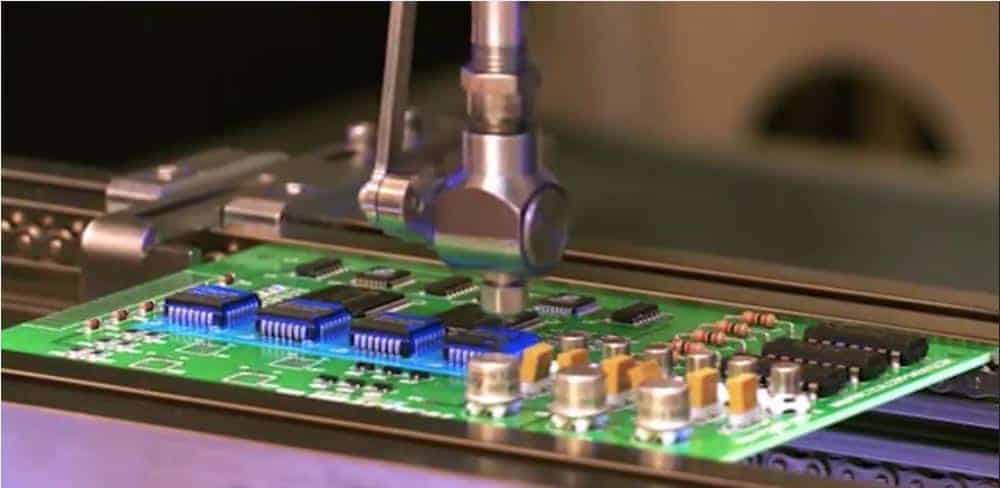
PCB Assembly
After the bare PCB is fabricated, the next phase is assembly (PCBA). This involves soldering surface mount (SMT) components and through-hole parts onto the board.
SMT Assembly
The steps in SMT assembly:
- Solder Paste Printing – Solder paste is printed on PCB pads using a stencil.
- Component Placement – Robots place tiny SMT parts onto the solder paste.
- Reflow Soldering – The board passes through a reflow oven. The solder paste melts, forming solder joints.
Key process parameters like paste deposition, placement accuracy, and thermal profiling must be tightly controlled.
Through-Hole Assembly
Leaded components like connectors are inserted into plated through-holes and soldered. Wave soldering immerses the bottom side of the board in molten solder. For through-hole on double-sided boards, selective hand soldering is required.
Cleaning
Post-soldering cleaning removes flux residue. Aqueous washing and semi-aqueous processes are commonly used.
Inspection and Testing
Quality control steps like optical inspection and board functional tests are critical to ensure product reliability:
- X-Ray Inspection – Detects solder defects and foreign objects.
- In-Circuit Test (ICT) – Tests circuit functionality.
- Flying Probe – Tests connectivity between test points.
Repairs and rework are done before final testing.
PCB Manufacturing Factors
Here are some key considerations when manufacturing PCBs:
- Lead Times – Can range from 24 hours for quick-turns to 4+ weeks for complex boards.
- Quality – Look for certification (ISO 9001, IPC, UL), quality processes, equipment technology.
- Capabilities – Evaluate services offered, maximum board size, layer count, line widths, volumes.
- Cost – Depends on board complexity, layer count, size, volume, lead time.
- Supply Chain – Ensure stable supply of materials, avoid long fulfillment times.
- IP Protection – Some companies offer NDA and secure data transfer options.
Reputable PCB manufacturers provide design for manufacturing (DFM) feedback to avoid manufacturability issues. Working closely with your PCB partner ensures a smooth production process and high-quality boards.
Conclusion
Manufacturing reliable, high-performance PCBs requires expertise across complex processes from imaging and etching to soldering and inspection. Withiterative design, strict process controls, quality components, and thorough testing, PCB fabricators can deliver boards that meet the demands of electronic products. This guide covers key considerations in PCB materials, fabrication, assembly, testing, and procurement to help successfully produce your next printed circuit board design.
Frequently Asked Questions
What are the most common PCB materials?
The most common PCB substrate is FR-4, a glass-reinforced epoxy. Other materials include ceramics like alumina, polyimides for flex boards, and metal cores. Copper foils, soldermasks, and prepregs are also important materials.
How are multilayer PCBs fabricated?
Multilayer PCBs interleave laminated substrate and prepreg layers. Copper layers are imaged, etched, and stacked up. Lamination under heat and pressure bonds the layers into a single board with electrical connections between layers through plated vias.
What is the difference between wet etching and dry etching?
Wet etching uses liquid chemicals like ferric chloride to remove unwanted copper. Dry etching uses plasma to sputter away copper. Wet etching is faster and cheaper but has chemical waste. Dry etching is more precise and eco-friendly.
What are the main steps in SMT assembly?
SMT assembly includes solder paste printing, robotic component placement, and reflow soldering in an oven to form solder joints. Process control parameters like paste deposition and thermal profiling are critical.
How is PCB quality and reliability ensured?
Extensive inspection, testing, and quality control steps are implemented. Optical and x-ray inspection, ICT testing, and flying probes verify solder joints, component placement, continuity, and board function. ISO certification and process audits also guarantee quality.


0 Comments