A Printed Circuit Board (PCB) stackup refers to the specific arrangement and sequence of various layers that make up a PCB. It is a crucial aspect of PCB design, as it determines the electrical and mechanical properties of the board, as well as its performance and reliability. The stackup defines the number of conductive layers, the materials used for each layer, and their respective thicknesses and positions within the board.
PCB stackups are designed to meet the requirements of the electronic circuit, taking into account factors such as signal integrity, power distribution, thermal management, and mechanical robustness. The complexity of the stackup can vary widely, ranging from simple single-layer or double-layer boards to highly complex multi-layer boards with dozens of conductive layers.
Importance of PCB Stackup Design
The PCB stackup design plays a critical role in the overall performance and functionality of the electronic device or system. A well-designed stackup can:
- Ensure signal integrity: By carefully arranging and separating signal layers, power planes, and ground planes, the stackup can minimize electromagnetic interference (EMI), crosstalk, and other signal integrity issues.
- Optimize power distribution: Proper placement of power and ground planes can provide efficient power distribution and minimize voltage drops, ensuring stable and reliable power delivery to the components.
- Enhance thermal management: The materials used in the stackup, such as thermally conductive layers or prepregs, can help dissipate heat generated by high-power components, preventing overheating and improving the overall reliability of the system.
- Improve mechanical strength: The stackup design can incorporate rigid or flexible materials, reinforcements, or specialized cores to provide the required mechanical strength and flexibility for the intended application.
- Facilitate high-speed signal transmission: For high-speed digital circuits or radio frequency (RF) applications, the stackup can be optimized to support controlled impedance and minimize signal reflections and losses.
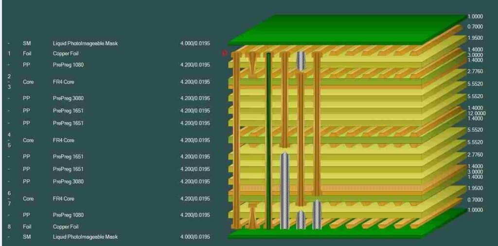
Components of a PCB Stackup
A typical PCB stackup consists of the following components:
- Conductive layers: These are the copper layers that carry signals, power, and ground connections. They can be signal layers, power planes, or ground planes.
- Dielectric layers: These are insulating layers, typically made of materials like FR-4, polyimide, or other reinforced resins, that separate and insulate the conductive layers.
- Prepregs: Prepregs (pre-impregnated fiberglass reinforcements) are used to bond the conductive and dielectric layers together, providing mechanical strength and dimensional stability.
- Core: The core is the central layer or set of layers in a multi-layer PCB, typically made of a rigid or flexible material, depending on the application.
- Solder mask: This is a thin protective layer applied over the outer conductive layers, leaving openings (pads) for component mounting and soldering.
- Surface finishes: These are coatings applied to the exposed conductive surfaces (e.g., pads, vias) to facilitate soldering, prevent oxidation, and enhance surface planarity.
Types of PCB Stackups
PCB stackups can be categorized based on various criteria, such as the number of layers, materials used, and the intended application. Here are some common types of PCB stackups:
- Single-layer or double-layer stackups: These are the simplest stackups, consisting of one or two conductive layers separated by a dielectric layer.
- Multi-layer stackups: These stackups have three or more conductive layers, allowing for more complex circuitry and better signal integrity.
- Rigid PCB stackups: These stackups are made of rigid materials, such as FR-4 or polyimide, and are suitable for applications that require mechanical strength and durability.
- Flexible PCB stackups: These stackups incorporate flexible materials, like polyimide or liquid crystal polymer (LCP), and are designed for applications that require bendability or flexibility.
- High-frequency or RF stackups: These stackups are optimized for high-frequency or radio frequency applications, employing materials with low dielectric constants and controlled impedance layers.
- High-power or thermal stackups: These stackups incorporate thermally conductive materials, such as aluminum or specialized prepregs, to facilitate heat dissipation and improve thermal management.
- Embedded component stackups: These stackups include embedded components, such as resistors, capacitors, or even active devices, directly integrated into the PCB layers, resulting in a more compact and efficient design.
PCB Stackup Design Considerations
When designing a PCB stackup, several factors must be taken into account to ensure optimal performance and reliability. Some key considerations include:
- Signal integrity requirements: The stackup should be designed to minimize signal reflections, crosstalk, and other signal integrity issues, particularly for high-speed or high-frequency applications.
- Power distribution and management: The placement and design of power planes and ground planes should ensure efficient power delivery and proper decoupling of power and ground connections.
- Thermal management: The stackup should incorporate materials and design elements that facilitate heat dissipation, especially for high-power or densely populated boards.
- Mechanical requirements: The stackup should provide the necessary mechanical strength, rigidity, or flexibility based on the application’s requirements, such as handheld devices, wearable electronics, or automotive applications.
- Manufacturing considerations: The stackup design should take into account the manufacturing capabilities, materials availability, and cost constraints to ensure feasibility and cost-effectiveness.
- Regulatory compliance: Certain applications, such as aerospace, military, or medical devices, may have specific regulatory requirements that influence the stackup design and material selection.
- Design for testability and rework: The stackup should accommodate testability and rework considerations, such as the inclusion of test points, access to buried vias, and the ability to remove and replace components.
PCB Stackup Design Tools and Simulation
To ensure optimal PCB stackup design, engineers often rely on specialized software tools and simulation techniques. These tools can help analyze and validate the stackup design before physical prototyping, reducing the need for costly iterations and improving overall design efficiency.
- PCB design software: Most PCB design software packages, such as Altium Designer, Cadence Allegro, or Mentor Graphics, include stackup design tools and libraries for various materials and stackup configurations.
- Signal integrity simulation: Tools like HyperLynx, Ansys SIwave, or Cadence Sigrity can simulate and analyze signal integrity issues, such as crosstalk, reflections, and impedance mismatches, based on the stackup design.
- Thermal simulation: Thermal simulation tools, like Mentor Graphics FloTHERM or Ansys Icepak, can model and predict the thermal behavior of the PCB stackup, allowing for optimizations in heat dissipation and thermal management.
- Mechanical simulation: Finite element analysis (FEA) tools, such as Ansys Mechanical or Siemens NX Nastran, can simulate the mechanical stress, deformation, and vibration characteristics of the PCB stackup under various loading conditions.
- Electromagnetic simulation: Tools like Ansys HFSS or Cadence Clarity 3D Solver can simulate and analyze the electromagnetic behavior of the PCB stackup, particularly for high-frequency or RF applications.
By leveraging these tools and simulation techniques, engineers can iterate and refine the PCB stackup design, ensuring that it meets the desired electrical, thermal, and mechanical performance requirements before committing to physical prototyping and manufacturing.
Table: Common PCB Stackup Materials
| Material | Dielectric Constant (Dk) | Loss Tangent (Df) | Typical Applications |
|---|---|---|---|
| FR-4 | 4.0 – 4.7 | 0.02 – 0.03 | General-purpose PCBs |
| Polyimide | 3.4 – 3.8 | 0.002 – 0.008 | Flexible PCBs, high-frequency applications |
| Rogers RO4003C | 3.38 | 0.0027 | High-frequency, RF/microwave applications |
| Isola IS680 | 4.0 | 0.016 | High-speed digital, low-loss applications |
| Aluminum | N/A | N/A | High thermal conductivity, power electronics |
| Copper | N/A | N/A | Power planes, ground planes, signal layers |
Table: Common PCB Stackup Configurations
| Configuration | Description | Typical Applications |
|---|---|---|
| Single-layer | One conductive layer on one side of the dielectric | Simple circuits, prototypes, low-cost applications |
| Double-layer | Two conductive layers separated by a dielectric | Basic analog and digital circuits, simple products |
| 4-layer | Four conductive layers (signal, power, ground, signal) | Medium complexity analog and digital circuits |
| 6-layer | Six conductive layers (signal, ground, power, power, ground, signal) | High-density analog and digital circuits |
| 8-layer | Eight or more conductive layers | High-complexity circuits, signal integrity-critical applications |
| Rigid-flex | Combination of rigid and flexible layers | Wearable devices, handheld electronics, aerospace |
| High-frequency | Low-loss materials, controlled impedance layers | RF/microwave circuits, high-speed digital applications |
| High-power | Thermally conductive layers, thick copper planes | Power electronics, motor drives, high-current applications |
Frequently Asked Questions (FAQ)
- What is the purpose of a PCB stackup? The purpose of a PCB stackup is to define the arrangement and sequence of various layers that make up a printed circuit board. It determines the electrical, thermal, and mechanical properties of the board, ensuring optimal performance and reliability for the intended application.
- How does the PCB stackup affect signal integrity? The PCB stackup plays a crucial role in signal integrity by controlling the placement and separation of signal layers, power planes, and ground planes. Proper stackup design minimizes electromagnetic interference, crosstalk, and signal reflections, ensuring clean and reliable signal transmission.
- Why is thermal management important in PCB stackup design? Thermal management is essential in PCB stackup design, especially for high-power or densely populated boards. The stackup should incorporate materials and design elements that facilitate heat dissipation, such as thermally conductive layers or specialized prepregs, to prevent overheating and improve overall reliability.
- What are the common materials used in PCB stackups? Common materials used in PCB stackups include FR-4 (general-purpose), polyimide (flexible and high-frequency), Rogers RO4003C (high-frequency), Isola IS680 (low-loss), aluminum (high thermal conductivity), and copper (conductive layers).
- How do PCB stackup design tools and simulations help in the design process? PCB stackup design tools and simulations allow engineers to analyze and validate the stackup design before physical prototyping. They can simulate and predict signal integrity, thermal behavior, mechanical stress, and electromagnetic characteristics, enabling design optimizations and reducing the need for costly iterations.
By understanding the PCB stackup and its importance in PCB design, engineers can create high-performance, reliable, and cost-effective electronic products that meet the desired specifications and requirements.CopyRetry


0 Comments