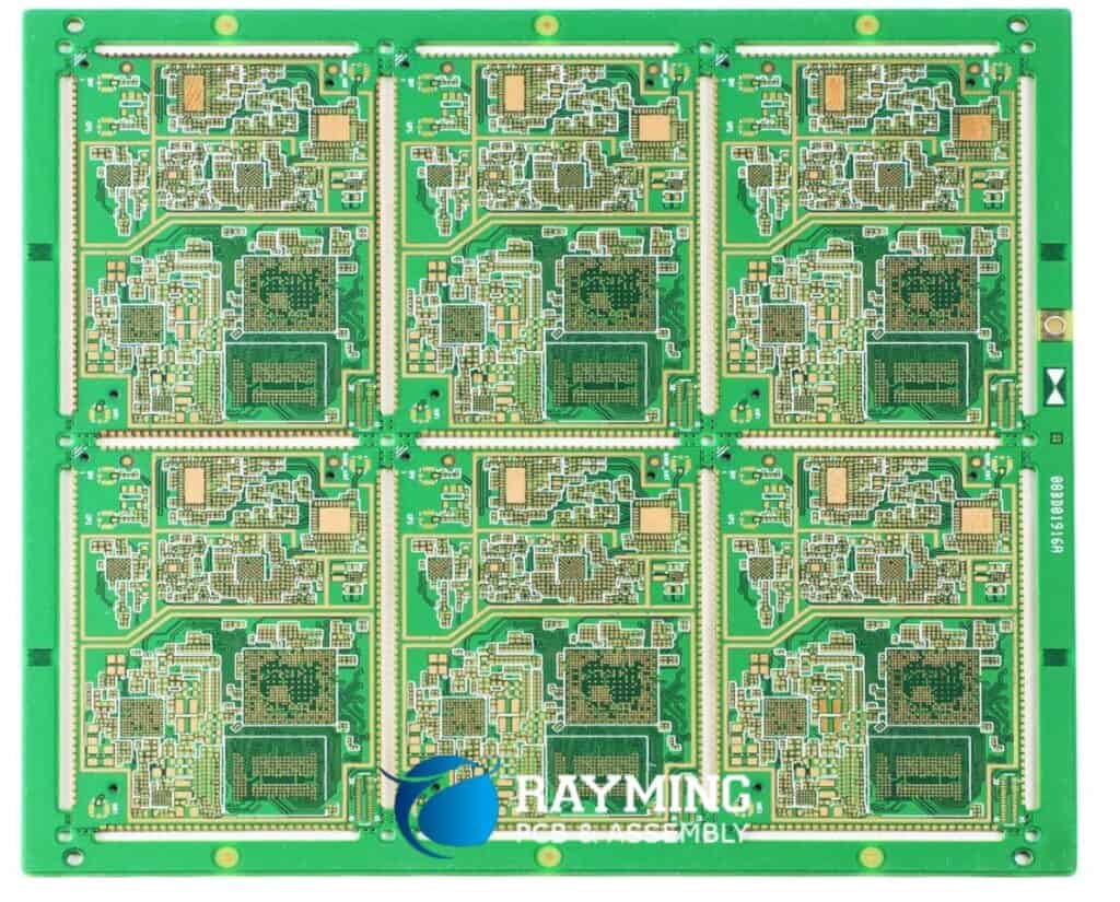
Printed circuit boards (PCBs) constitute the core foundation of electronics that powers modern technological advancements. PCBs undergo tremendous complexity in manufacturing specialized multi-layer boards that interconnect and package electronic components.
PCB fabrication facilities known as “PCB fabs” handle this sophisticated process of transforming raw base materials into fully assembled boards ready for integration into products. They leverage cutting-edge capabilities spanning board fabrication, component assembly, and testing under tightly controlled environments.
This article will provide a comprehensive overview of PCB fabs covering:
Role of PCB Fabs
A PCB fab refers to the manufacturing facility focused on volume production of printed circuit boards following customer requirements. They are high-tech workshops specialized in PCB fabrication and assembly aimed toward reliability, quality, efficiency and cost targets.
PCB fabs transform design files and electrical requirements into physical boards ready for deployment across diverse applications like consumer electronics, medical systems, aerospace, automotive, etc. This involves everything from documentation to final testing and logistics.
Capabilities encompass engineering collaboration through manufacturing processes within cleanroom environments and stringent process controls to guarantee performance.
Types of PCB Fabs
There exist two primary varieties of PCB fabrication units:
Integrated Device Manufacturers (IDM)
IDMs refer to companies that design and sell complete electronic devices like Intel, Samsung, etc. They own internal PCB fabrication facilities to cater exclusively to their product needs from chip packaging to boards.
Optimized for their proprietary use cases, IDMs prioritize protection of intellectual property (IP), maintaining in-house control, and aligning roadmaps between divisions. But capacities remain focused on captive requirements.
Merchant Manufacturers
Merchant fabs constitute independent PCB manufacturing centers providing fabrication and assembly services to a broad customer base. Ranging from large conglomerates like Flex, Jabil Circuits, Sanmina to smaller specialty houses, they cater to diverse industry segments.
They operate on an outsourced production basis focused on quality, affordability and quick turnarounds. Investments continuously upgrade capabilities anticipating emerging needs. Competencies cover everything from single boards to highly dense multi-layer PCBs.
Here is a comparison:
| Parameter | IDM Fabs | Merchant Fabs |
|---|---|---|
| Ownership | Internal part of device company | Independent board production |
| Focus | Captive use | Broad outsourced fabrication |
| Breadth | Limited segments | Diverse technologies/volumes |
| Flexibility | Aligned to company roadmap | Customizable services |
Merchant fabs dominate the PCB supply chain owing to specialization benefits.
Overview of PCB Manufacturing Process
PCB fabs facilitate everything from the initial electrical concepts through various stages ultimately achieving a functioning board product.
Design and Layout
- Schematics get drawn, boards get architected in CAD
- Component selection, trace routing, stackups, placements defined
- Testing points provisioned, panelization planned
This design packaging ensures the board can achieve desired functionality and performance.
Fabrication
- Layers of conductive copper foil sandwich insulating dielectric
- Chemical processes transfer images, etch conductors
- Physical drilling forms vias between layers
- Various finishes and coatings apply through plating, deposition
These steps transform base materials into patterned laminates with all conductive interconnections between components.
Assembly
- Components get mounted and soldered onto boards
- Leaded components inserted or surface mounts reflowed
- Adhesives, encapsulations, conformal coatings protect parts
- Post-assembly inspection and touchup occurs
This results in fully loaded PCB assemblies integrating components.
Testing
- Electrical validation happens through in-circuit testing
- Functional system level tests execute
- Environmental stress screening shakes out defects
- X-ray and optical inspection ensure quality
Stringent testing provides quality assurance checks before customer shipments.
Required Fab Capabilities
Manufacturing PCBs involves a tremendous diversity of processes requiring an equally broad set of specialized capabilities:
Equipment
Sophisticated PCB equipment encompasses:
- Photoplotters, film cameras for master imaging
- Etching machinery and handling for conductors patterning
- Complex multi-spindle drills
- Plating equipment like electrolytic copper plating
- Exposure units for applying photoimageable layers
- Wave, selective soldering units
- Testing/inspection systems
Facilities
Advanced fab facilities incorporate:
- Cleanrooms for assembly areas with controlled environments
- Exhaust management abating chemical effluents
- Deionized water production and distribution networks
- Material handling like automated guided vehicles (AGV)
- Lean production layouts balancing work flows
- Class 10000/Class 100 standards in critical zones
- Anti-static design and protection
These high-tech equipment and facilities handle intricate multi-layer board fabrication allowing miniaturization.
Operational Considerations for Efficient Fabs
Process capabilities mean little without optimizing operational metrics that directly impact manufacturability like cycle times, changeover overheads and yield rates.
Cycle Time
Cycle time defines the total duration a PCB experiences from initial inputs to processed outputs ready for shipping. This depends on:
- Number of setup, production, inspection steps
- Process durations across material handoffs
- Wait overheads between equipment batches
- Assembly soldering, cleaning sequences
Tracking cycle time bottlenecks help streamline flows. Average cycle times range from 48-72 hours currently.
Changeovers
Production changeovers when switching between PCB variants or reloading consumables affect uptime. Line stoppages trigger loss of sales. Steps include:
- Machine shutdown, materials unloading
- Reprogramming setup parameters
- Test production post changeover
- Process tuning to hit tolerances
Quick turnaround changeovers minimize downtimes enabling flexible operations.
Yields
A key metric like process yield directly impacts the usable boards output driving profits. This encompasses:
- Bare board fabrication yield factors
- Reliability affected boards after assembly
- Test failures rejecting boards
- Process defects like handling damages
Improving yields through process capability, quality control, prevents waste.
Here is a summary view:
| Metric | Importance | Sample Range |
|---|---|---|
| Cycle Times | Customer responsiveness | 48-72 hours |
| Changeover Time | Production flexibility | <1.5 hours |
| Yields | Process stability | >98% |
These operational aspects separate elite ultra-efficient PCB fabs meeting demands.
Certifications and Compliance
Given extensive chemical processing and handling of sophisticated materials in PCB manufacturing, fabs require several certifications including:
- IPC Standards: Fabrication/assembly workmanship adhering to IPC classes
- ISO: International Organization for Standardization compliance for quality management like ISO 9001
- Environmental: Following management standards like ISO 14001
- ITAR Registration for restricted defense/aerospace work
- Axia Best Practices focusing on social responsibility
Many of these validate capabilities through audits of procedures, facilities, final test data and results. Maintaining multiple authentications allows fabs to diversify across market verticals through demonstrated accountability.
Conclusion
PCB fabs transform design concepts into functioning board realities following stringent fabrication and assembly processes. Specialized equipment and optimized facilities handle PCB manufacturing bridging initial ideas to final shipment.
Certified metrics across cycle times, changeovers and yields coupled with responsible operational practices manifest the capacities separating leading fabrication facilities. Technological proficiency and reliable quality built through process repeatability, expertise allows fabs to drive innovation fulfilling present and emerging electronics needs.
Frequently Asked Questions
How are PCB fabs different from PCB assembly service providers?
PCB fabs provide complete fabrication through assembly offering:
- Base materials preparation
- Imaging, etching, drilling steps
- Plating, coating, legend printing
- Soldering components onto boards
- Conformal coatings, potting
Assemblers only mount components onto supplied boards.
What core expertise separates merchant PCB fabs from IDMs?
Merchant fabs specialize around:
- Diverse technology breadth across industry verticals
- Customer focused services and rapid prototyping
- Adaptability toward emerging fabrication needs
- Quality benchmarking through certifications
How do PCB fabs minimize changeover time overheads?
Methods to reduce changeover times when switching production include:
- Standardized procedures with checklists
- Quick change custom tools
- Pre-setup of machine parameters
- Parallel activities during change window
What process optimizations maximize PCB fab yields?
Improving yields involves:
- Stringent process control limits
- Gauging capability indices (Cpk/Ppk)
- Monitoring defects and pareto analysis
- SPC control charts to eliminate variables drift
How critical is an environmentally responsible framework for PCB fabs?
Environmental sustainability through certified ISO 14001 policies helps by:
- Ensuring chemical/waste legal compliance
- Promoting recycling and conservational initiatives
- Reducing energy consumption and emissions
- Auditing carbon footprint


0 Comments