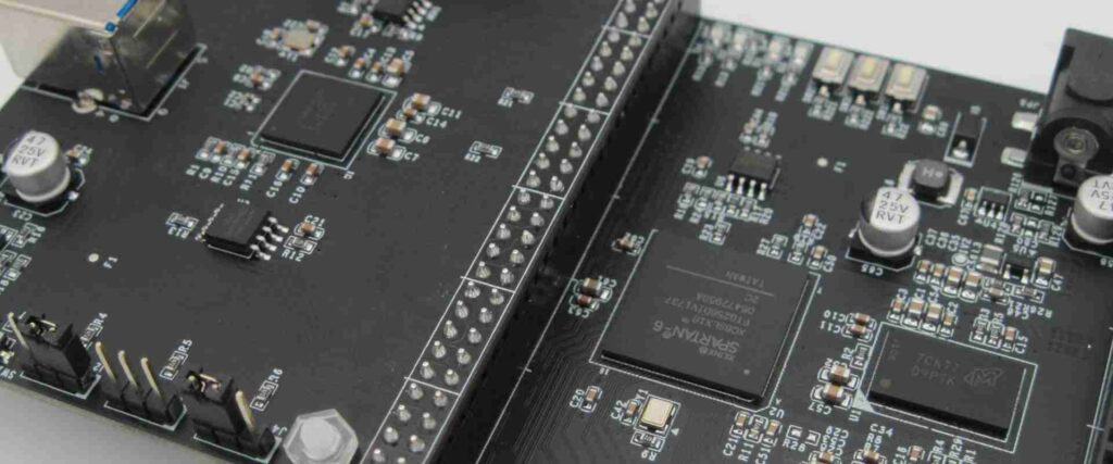
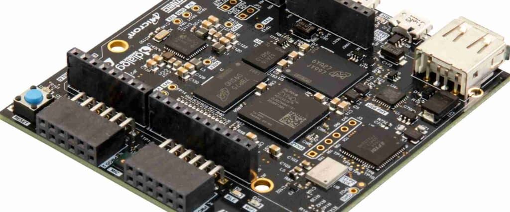
What are Assy PCBs?
An assy PCB, short for assembled printed circuit board, refers to a PCB that has electronic components already soldered and assembled on it. While bare PCBs contain just the copper traces and holes, assy PCBs are fully populated with the required components to function.
Some key benefits of using assy PCBs include:
- Faster production – With components already assembled, assy PCBs let you quickly integrate them into your products. You avoid the time-consuming soldering and assembly process.
- Specialized skills not needed – Assy PCBs eliminate the need for skilled soldering and assembly technicians on your team. The PCB manufacturer handles the component population for you.
- Improved quality – PCB assembly is best left to specialized manufacturers with the right tools and processes. They can ensure high-quality solder joints and reliable component placement.
- Cost-saving – For low to medium production volumes, getting fully assembled PCBs can be cheaper than doing in-house assembly. The costs are lowered due to the economy of scale at the PCB assembly house.
Types of Assembled PCBs
There are a few variances when it comes to assembled PCBs:
1. Full Assembly vs Partial Assembly
Fully assembled PCBs have all required components populated on them. Partially assembled PCBs may just have the most difficult portions assembled, like BGA chips and QFN components. The easier portions are left for manual assembly.
2. Through-Hole Assembly vs SMT Assembly
Through-hole PCB assembly refers to the installation of leaded components in holes on the PCBs. SMT or surface mount assembly means soldering surface mount devices onto pads on the outer surfaces. Most modern assy PCBs use SMT assembly exclusively.
3. Single-sided vs Double-sided Assembly
Single sided assembly means all components are placed on only one side of the PCB. Double-sided has components mounted on both sides. Double-sided packing allows higher component density.
4. Standard vs Complex Assembly
Standard assembly has common component types and PCB specs. Complex assembly involves advanced component types like MCMs, RF shields, or large multi-row connectors. It needs specialized assembly processes.
5. Low vs High Mix Assembly
Low mix PCBs involve assembling multiple identical PCBs. High mix means frequently changing between different PCB designs in short production runs. High mix increases changeover processes.
Assy PCB Assembly Process Step-by-Step
Here is a look at a typical end-to-end assembly process flow when ordering fully loaded assy PCBs:
1. Design Files
The first step is providing the PCB and bill of materials (BOM) files to the assembly house. Gerber, NC drill, centroid data, Pick and Place (PNP) files, assembly drawings, and component datasheets are also shared.
2. Kitting
The manufacturer does component kitting by sourcing all the required parts listed in the BOM. Missing or incorrect parts are flagged to the customer.
3. Solder Paste Stenciling
A solder stencil is created by laser cutting or chemical etching. Solder paste is applied through the stencil openings onto the PCB pads.
4. Pick and Place
Components are precisely picked from feeders and placed onto the solder paste by advanced PNP machines. Vision alignment, force control, and accuracy levels in microns are ensured.
5. Reflow Soldering
The PCB passes through a reflow oven to heat up. The solder paste melts, solders the components, and secures them to the board.
6. Optical Inspection
Automated optical inspection (AOI) checks for defects like misalignments, missing parts, tombstoning, etc. Errors are flagged for rework.
7. Testing and QC
Programming, functional testing, and quality checks confirm assemblies match design specs. Failed boards are debugged and reworked.
8. Conformal Coating
A protective plastic coating may be sprayed onto the assembled boards for environmental protection.
9. Final Packaging
The finished assy PCBs go through anti-static bagging or vacuum sealing before shipment.
Factors to Consider When Ordering Assy PCBs
Here are some key considerations when getting assembled PCBs made:
Choose the Right PCB Assembly House
Select an assembly partner with expertise in your type of product. Audit their production facility, processes, and quality certifications.
Provide Detailed and Accurate Design Files
Ensure your Gerber, BOM, centroid, assembly drawings are complete and error-free. Missing data will delay orders.
Include a PCB Test Plan
Provide test procedures or furnish functioning golden boards to program test fixtures. Communicate the required acceptance criteria.
Determine Testing Needs Upfront
Decide on the level of component programming, in-circuit testing, functional validation, burn-in, and inspection. This impacts costs.
Plan for Design Re-spins
Schedule time and budget for potential re-spins if the first assembled boards need design modifications.
Estimate Realistic Lead Times
Assembly lead times vary from 2 days to 4 weeks based on production loads, complexity, and components sourced.
Review Quality Standards
Agree on quality metrics like IPC Class 2 or Class 3 requirements. More stringent requirements increase costs.
Scale your Orders Economically
Carefully plan order quantities based on demand. Balance cost savings from volume orders with inventory holding costs.
How to Design PCBs for Easier Assembly
Here are some PCB design guidelines to enable low-cost, high-yield assembly:
Component Selection
- Select surface mount device packages suited for automated assembly like SOICs, QFNs, 0402 discretes.
- Avoid connectors, switches, or odd-form components incompatible with SMT lines.
- Design with standard components from approved vendor lists available at assembly houses.
- Check component pad dimensions against manufacturer recommendations.
- Place components with the assembly process in mind. Group common parts together.
- Ensure sufficient clearance between adjacent parts for pick and place vacuum nozzles.
- Include fiducial marks to help with vision alignment during assembly.
- Add sufficient test points for validation and debugging after assembly.
- Eliminate unused pads which can cause placement confusion.
Solder Mask Design
- Avoid solder mask defined (SMD) pads. Use NSMD pads with larger openings than metal pads.
- Don’t fully tent vias. Provide solder openings for via barrel fills.
- NSMD pads ease inspection of solder joints.
- Ensure reference designators match the BOM ordering.
- Place polarity indicators correctly next to polarized parts.
- Provide visual assembly guides like component placement outlines.
Board Outline and Features
- Include board handling features like rails, holders, fiducials for assembly jigs.
- Provide sufficient board spacing for clamping during soldering.
- Tooling holes help alignment during population.
- Breakaway tabs let PCB panels be separated post-assembly.
<style type=”text/css”> .tg {border-collapse:collapse;border-spacing:0;} .tg td{border-color:black;border-style:solid;border-width:1px;font-family:Arial, sans-serif;font-size:14px; overflow:hidden;padding:10px 5px;word-break:normal;} .tg th{border-color:black;border-style:solid;border-width:1px;font-family:Arial, sans-serif;font-size:14px; font-weight:normal;overflow:hidden;padding:10px 5px;word-break:normal;} .tg .tg-c3ow{border-color:inherit;text-align:center;vertical-align:top} </style> <table class=”tg”> <thead> <tr> <th class=”tg-c3ow”><b>SMD Package Types</b></th> <th class=”tg-c3ow”><b>Description</b></th> <th class=”tg-c3ow”><b>Assembly Notes</b></th> </tr> </thead> <tbody> <tr> <td class=”tg-c3ow”>SOIC</td> <td class=”tg-c3ow”>Small outline integrated circuit package</td> <td class=”tg-c3ow”>Very assembly friendly</td> </tr> <tr> <td class=”tg-c3ow”>QFN</td> <td class=”tg-c3ow”>Quad flat no-lead package</td> <td class=”tg-c3ow”>Require paste printing for underneath pads</td> </tr> <tr> <td class=”tg-c3ow”>0402</td> <td class=”tg-c3ow”>Rectangular passive component size</td> <td class=”tg-c3ow”>Very small, need fine pitch assembly</td> </tr> <tr> <td class=”tg-c3ow”>0603</td> <td class=”tg-c3ow”>Rectangular passive component size</td> <td class=”tg-c3ow”>Recommended smallest size</td> </tr> <tr> <td class=”tg-c3ow”>0805</td> <td class=”tg-c3ow”>Rectangular passive component size</td> <td class=”tg-c3ow”>Easy to assemble size</td> </tr> </tbody> </table>
Assy PCB Manufacturers to Consider
Here are some reputable printed circuit board assembly service providers to consider for your orders:<table class=”tg”> <thead> <tr> <th class=”tg-c3ow”><b>Company</b></th> <th class=”tg-c3ow”><b>Location</b></th> <th class=”tg-c3ow”><b>Volume Capabilities</b></th> </tr> </thead> <tbody> <tr> <td class=”tg-c3ow”>Elecrow</td> <td class=”tg-c3ow”>China</td> <td class=”tg-c3ow”>Medium to high volumes</td> </tr> <tr> <td class=”tg-c3ow”>PCBWay</td> <td class=”tg-c3ow”>China</td> <td class=”tg-c3ow”>Low to medium volumes</td> </tr> <tr> <td class=”tg-c3ow”>Advanced Circuits</td> <td class=”tg-c3ow”>United States</td> <td class=”tg-c3ow”>Low to medium volumes</td> </tr> <tr> <td class=”tg-c3ow”>Sierra Circuits</td> <td class=”tg-c3ow”>United States</td> <td class=”tg-c3ow”>Low to medium volumes</td> </tr> <tr> <td class=”tg-c3ow”>Imagineering</td> <td class=”tg-c3ow”>United Kingdom</td> <td class=”tg-c3ow”>Low to medium volumes</td> </tr> </tbody> </table>
Do your due diligence to pick the right assembly partner based on capabilities, quality, lead times and costs. Get assembled samples done before committing to a full production order.
FQA About Assembled PCBs
Q: Why are assembled PCBs more expensive than bare PCB boards?
A: The assembly process of soldering components has additional costs. These include expenses for solder paste, stencils, advanced PNP machines, skilled operators, soldering ovens, inspection systems, testing, debugging, and overhead costs.
Q: Can I order 1-2 piece samples of an assembled PCB?
A: Most assembly houses have minimum order quantities starting at 3-5 pieces for assembled boards. This is because the fixed setup costs are high. Building jigs and programming for just 1-2 pieces is usually not economically feasible.
Q: How are components secured on double-sided assembled boards?
A: For double-sided SMT, adhesive is applied on one side. Components are placed on this glue and then soldered on the other side in the reflow oven. Some components may also be anchored using through-hole pins.
Q: What file formats do assembly houses need for manufacturing?
A: The Gerber, centroid, BOM, pick and place, assembly drawings, schematics, and component datasheets need to be provided. These should be in the native CAD file formats used.
Q: Can assembled PCBs be reworked and modified?
A: Yes, rework using soldering irons is possible for minor modifications. But extensive changes become uneconomical versus assembling a fresh version. For high-volume products, it’s recommended to get assembled samples fully correct before starting production.
Conclusion
Assy PCBs with pre-assembled components offer engineers a fast and easy option compared to DIY assembly. They allow focusing on core product development rather than manufacturing aspects. For high-quality assembled boards delivered on schedule, carefully select an assembly house and provide comprehensive design files. Investing effort in designing assembly-friendly PCB layouts right from the start yields dividends in the long run through smoother assembly, testing, and servicing.


0 Comments