Surface mount technology (SMT) is a method of producing electronic circuits where components are mounted directly onto the surface of printed circuit boards (PCBs). This manufacturing process has largely replaced the traditional through-hole technology and has enabled further miniaturization of electronics. In this article, we will explore the key steps involved in SMT production.
SMT Component Preparation
The first stage of the SMT production process is component preparation. This involves procuring the surface mount devices (SMDs) or components and packaging them for ease of handling by the pick-and-place machines.
Some key aspects include:
Sourcing and Procurement
- Components may be sourced directly from manufacturers or via authorized distributors. Key factors considered during sourcing include quality, reliability, lead times, and costs.
Taping and Reeling
- Most SMDs are packaged in tapes or reels for automatic feeding during assembly. The tapes and reels hold multiple identical components aligned sequentially.
- Taping involves placing components in specially designed pockets embossed on carrier tapes and sealing with cover tape. Reels wind the taped components for storage and transportation.
Traying
- Larger or heavier SMDs like BGAs and connectors that won’t work with tapes/reels are placed in trays. The trays have pockets or cavities to hold individual components.
Dry Packing
- Moisture sensitive components need to be sealed in dry bags or containers with desiccants to prevent moisture absorption and damage.
SMT Stencil Preparation
The solder paste stencil is a thin metal sheet that transfers solder paste onto the PCB pads during printing. Its preparation includes:
- Design and fabrication – Stencils are designed with openings that match the copper pads on the PCB. Lasers cut these openings into the stencil.
- Cleaning and maintenance – Stencils are cleaned regularly using isopropyl alcohol to remove solder residue. This helps maintain printing accuracy and quality.
- Stencil storage – After cleaning, stencils are placed in storage racks or frames to avoid warpage.
Solder Paste Printing
Solder paste printing deposits the solder paste that bonds components to the PCB. Key steps are:
- The stencil is aligned and clamped onto the PCB.
- Solder paste is dispensed along one edge of the stencil.
- A squeegee blade spreads the paste across the stencil, forcing it through openings onto pads.
- The stencil is then released and removed.
- This results in solder paste deposited accurately on required pads.
- The process is automated using stencil printers for high volume production.
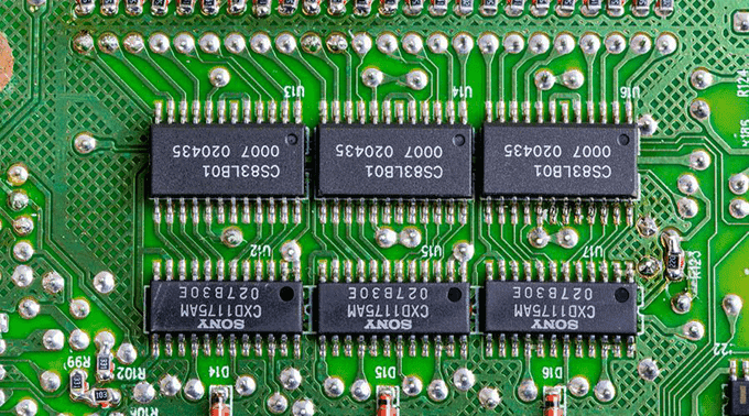
SMD Placement
SMDs are now placed on the solder paste using automated pick and place machines. The steps include:
- Machine setup – Feeders containing components are loaded on the pick-and-place head. Programs are uploaded.
- Paste inspection – Machines may optically inspect paste deposits and skip empty pads.
- Component placement – The head picks components from the feeders and places them accurately on the pads.
- Quality inspection – Placed parts may be inspected for alignment and orientation.
Reflow Soldering
Reflow soldering electrically and mechanically attaches the components to the PCB pads:
- The assembly passes through a reflow oven on a conveyor belt.
- Different temperature zones heat up the assembly gradually to the reflow temperature.
- The solder paste melts, creating solder joints that connect terminals to the pads.
- The assembly is then cooled down gradually to solidify the joints.
- Optimal temperature profiles ensure complete soldering without damaging components.
Inspection and Testing
Multiple inspections and tests are conducted including:
- Visual inspection under microscope to check for defects like shorts, opens, missing parts etc.
- X-ray inspection reveals hidden soldering defects.
- In-circuit testing checks electrical performance of assembled boards.
- Functional testing verifies that the board functions as intended.
This helps catch assembly issues early and prevents passage of defective boards to further production stages.
SMT Rework
In case defects are identified, rework of the affected components may be needed. Common SMT rework steps include:
- Removal of defective component using hot air, infrared heating or soldering irons.
- Site redress by cleaning the pads and applying fresh solder paste.
- Placement of new component and reflow soldering.
- Repaired boards are re-inspected before release.
Rework repairs faulty boards, improving yield.
Conformal Coating
As a final step, many assembled PCBs have a protective conformal coating applied.
- The coating layer adheres conformally over the components and board.
- It protects against moisture, dust, chemicals and temperature extremes.
- Common coating materials include acrylic, silicone, urethane and parylene.
- Application methods include spraying, dipping, brushing and vapor deposition.
This completes the SMT production process. Conformal coated boards are then packed and shipped to customers.
Major Advantages of SMT Production
- Higher component density enabling miniaturization
- Improved reliability due to absence of leads
- Lower assembly costs due to automation
- Faster production rates and changeovers
- Easier automation and assembly
SMT manufacturing continues to evolve with trends like higher density interconnects, smaller components, and more. Advancements in material science, machinery, inspection systems, and data analytics will further mature this critical production process.
Frequently Asked Questions
What are the key differences between SMT and through-hole PCB assembly?
The main differences are:
- SMT components have solder pads, not wire leads. Through-hole components have wire leads inserted in holes.
- SMT components sit directly on the board surface, while through-hole components are secured by leads attached underneath.
- SMT assembly involves solder paste printing, automated component placement, and reflow soldering. Through-hole assembly uses manual insertion and wave soldering.
- SMT enables greater miniaturization and component density compared to through-hole.
- SMT is more suitable for automation and high-volume production than through-hole.
What are some common SMT component defects?
Some typical SMT component defects include:
- Missing components
- Wrong components or orientation
- Tombstoning where a component lifts during soldering
- Insufficient solder and dry joints
- Solder bridges causing shorts
- Solder balls or satellite dots
- Damage like cracks or broken leads
How are very small SMT components handled?
Extremely small SMT components below 01005 size (0.4mm x 0.2mm) are known as ultra-fine pitch components. Their handling requires:
- High precision pick-and-place machines with microscope cameras.
- Special nozzles for gripping the micro components.
- Solder pastes engineered for ultra-fine printing.
- Package singulation techniques to avoid loss of tiny components.
- High magnification optical inspection.
How are BGA components assembled using SMT?
Ball grid array (BGA) components have solder balls underneath instead of leads. Their SMT assembly involves:
- Precisely depositing solder paste on pads corresponding to the ball pattern.
- Tack-on process to lightly attach the balls to paste deposits.
- Reflow soldering melts the paste to create solder joints.
- X-ray inspection is commonly used for detecting soldering defects.
Why is solder paste printing critical in SMT?
Solder paste printing is critical because:
- It determines the position and amount of solder deposited.
- Errors like insufficient paste, clogged stencil apertures affect later stages.
- The quality and precision of printing impacts solder joint integrity.
- The composition of solder paste must match the assembly and process needs.


0 Comments