SMT stands for “Surface Mount Technology” referring to a method of mounting electronic components onto the surface of printed circuit boards (PCB) rather than passing component leads through holes to solder on the opposite side. First appearing commercially in the 1960s, surface mount became widely adopted by the late 1980s.
With miniaturization trends packing more functionality into integrated circuits (IC) in ever-shrinking packages, surface mount processes utilize robotic pick-and-place assembly to accurately populate small component sizes at high volumes efficiently. Avoiding through-hole terminations allows components soldering directly onto dense pad arrangements beneath body envelopes.
We explore key attributes around SMT components, PCB fabrication considerations supporting surface mount, soldering techniques, inspection methods, and factors influencing manufacturing quality and process selection.
Characterizing SMT Components
Surface mount devices span a vast range of package styles from connectors to resistors to complex application-specific ICs covering nearly every component type. But common traits emerge:
Small and lightweight – Components measure just millimeters per side from the diminutive 01005 size passive chips up to fine ball grid array (BGA) packages with 1mm ball spacing packing over 1,000 contacts in a grid beneath. Low mass eases high speed pick-and-place.
Terminations underneath – Instead of wire leads exiting sides, surface mount contacts consist of conductive pads, edge castellations or solder balls protruding from the underside body interfacing to PCB landing patterns when assembled.
Prevailingrectangular profiles – To maximize PCB real estate usage, SMT parts utilize narrow elongated outlines with rows/grids of terminals distributed along bodies. Rectangles improve positional stability during reflow attachment.
Markings – Lasered or printed text indicates component model numbers, ratings, polarity, lot codes and lead numbers supporting reliable assembly, inspection and field servicing.
These SMT hallmarks contrast markedly from through hole parts allowing radical escalation in fabrication densities.
Benefits of SMT Assembly
Several advantages arise from utilizing surface mount components and board fabrication methods:
Size – With no through-hole requirements, components minimize to the bare silicon die size itself. This enables scaled down board dimensions.
Automation – Machinery placements of small uniform SMT bodies simplifies volume production using precision pick-and-place equipment and solder paste printing.
Speed – Smaller components with leadless interface speed up solder paste reflow attachment cycles and downstream wash processes compared to conventional wave soldering.
Density – Eliminating through holes removes routing barriers allowing component placement extremely close even stacked vertically, maximizing layout densities.
Reliability – Short traces to BGA balls underneath ICs with high contact counts minimizes parasitic inductance improving signal quality at high frequencies.
Cost – Small component sizes leverage latest highly automated semiconductor wafer fabrication achieving very low per unit costs at volume.
Together these strengths make surface mounting the standard approach adopted across nearly all contemporary PCB production scenarios apart from certain high power modules.
Land Pattern Design
To translate surface mount components into soldered board interfaces requires fabricating metalized landing patterns on the substrate bonding locations. Design choices balance manufacturing tolerances and reliability. Key elements include:
Pads – Copper pads provide sufficient area to anchor component leads to board layers while concentrating solder volume for thermal transfer and mechanical clinching strength. Thermal relief cutouts prevent extreme heat sinking from planes.
Solder Mask – Dielectric solder mask dynamically expands/constricts around pads during thermal excursions controlling solder bead coalescence keeping joints isolated during reflow attachment. Photoimageable coatings pattern SMT sites.
Surface Finishes – Pad metalization selects §OLD, ENIG, Immersion Silver or OSP coatings compatible with solder paste retaining good wetting through repeated reflows. Pads also accommodate pad printing.
Fiducials – Copper landing patterns integrate locating markings like circles or crosses to support optical coordination of pick-and-place equipment precisely positioning components without compounding placement errors across large boards.
Balancing spacing/clearances along with finish and geometry factors allows fabricating pads correctly interfacing parts.
PCB Considerations for SMT Assembly
To reliably support surface mounting requires tailored board stackup constructions and layout considerations:
Layer Counts – High density designs demand multilayer boards stacking dozen conductive layers internally routing signals needing isolation from other nets while retaining ground plane shields minimizing EMI.
Materials – Temperature excursions during solder reflow and coefficient of thermal expansion mismatches dictate material selections like low CTE thermoset laminates to prevent bowed warpage cracking interfaces or damaging components.
Board Dimensions – Fabrication processes balance handling printed circuit panels efficiently through assembly lines against maximizing board sizes to leverage larger components packing more function per costly PCB. Cutting panels minimizes material discard.
Legend Printing – Ink jet solder mask image printers mark component locations, ratings, polarities and other assembly details right onto board layers guiding operators during manual touchups supplementing automated optical inspection systems.
Adapting PCB technology and layouts follows component evolution ensuring surface mount methods succeed both manufacturing components then soldering into products reliably.
Solder Paste Printing
To anchor surface mount components onto landing patterns requires applying tiny solder paste bricks onto pads where leads terminate underneath packages. Reflow heat then melts these pre-forms into metallurgic joint connections. Dispensing methods include:
Stenciling – Laser cut metal foil masks with small cutouts mirroring pad geometries get aligned over boards. A squeegee blade presses paste forcing it through apertures onto pads below. Fast cycle times with volume coverage.
Jet Printing – Precision nozzles directly eject tiny droplets only onto required pads sites eliminating stencils. Lower volumes but supports rapid changes dispensed accurately onto boards with extreme layout densities.
Dispensing – Needle dispenses paste points only where needed through CAM generated coordinate programs. Allows very precise volumes for thickness sensitive components but slower overall.
Printing processes cater towards SMT volumes and pad arrangements where small wells of solder paste adhere securing component placement until finalized under reflow heat into solder joints.
SMT Component Placement
Solving the logistical puzzle positioning thousands of tiny surface mount parts across large circuit boards falls upon high speed pick-and-place machines expertly optimizing mounting sequences Accuracy relies on:
Feeders – Components stored in tape/reels or tray cartridges get loaded into feeder slots choreographing selections inserting into pick positions awaiting retrieval by vacuum nozzles.
Nozzles – Computerized mechanisms collect parts from feeders and transfer towards board targets following programmatic trajectories then precisely drop components and retract awaiting next cycle. Nozzle types suit part geometries.
Boards – Servo table stages step boards methodically underneath placement heads incrementing once insertions finish in one region before nozzle cameras acquiring next location targets off loaded from feeders continue population until all sites across panels placed.
Inspection – Optical systems validate pad occupancies checking for missing or shifted components after placements verifying assemblies match programmed expectations before solder reflow occur integrating process feedback monitoring quality.
This orchestrated ballet of machinery swapping myriad tiny components from reels into PCBs underlies modern electronics assembly with accuracy and repeatability impossible manually.
SMT Solder Reflow Methods
With accurate pads printing and components populating boards, depositing heat melts solder pastes fusing surface tension into metallurgical bonds clinching parts onto circuit boards. Controlled ovens progression:
Preheat – Bottom IR heaters gently raise board and components to around 150°C expanding solder powder and slowly evaporating binder residues preparing solder and surfaces for wetting.
Soak – Convection heat saturates boards between 150°C to 200°C activating flux while balancing widget temperature gradients that otherwise risk deformations if uneven heating.
Reflow – Peak zone applies sharp rising slope from 200°C to 250°C sustaining just over 30 seconds adequately liquefying solder fully wetting pads as capillary forces draw molten droplets into coalesced joints ultimately anchoring components merged onto boards once cooled.
Cool Down – Moving boards from reflow into unpowered zones allows gradual solidification of solder re-crystallizing into hardened joints with light non stirred airflow and heat sinks preventingwarp distortions.
This thermal profile “bakes” assemblies setting components joined securely onto circuit boards through accurately formed solder bonds.
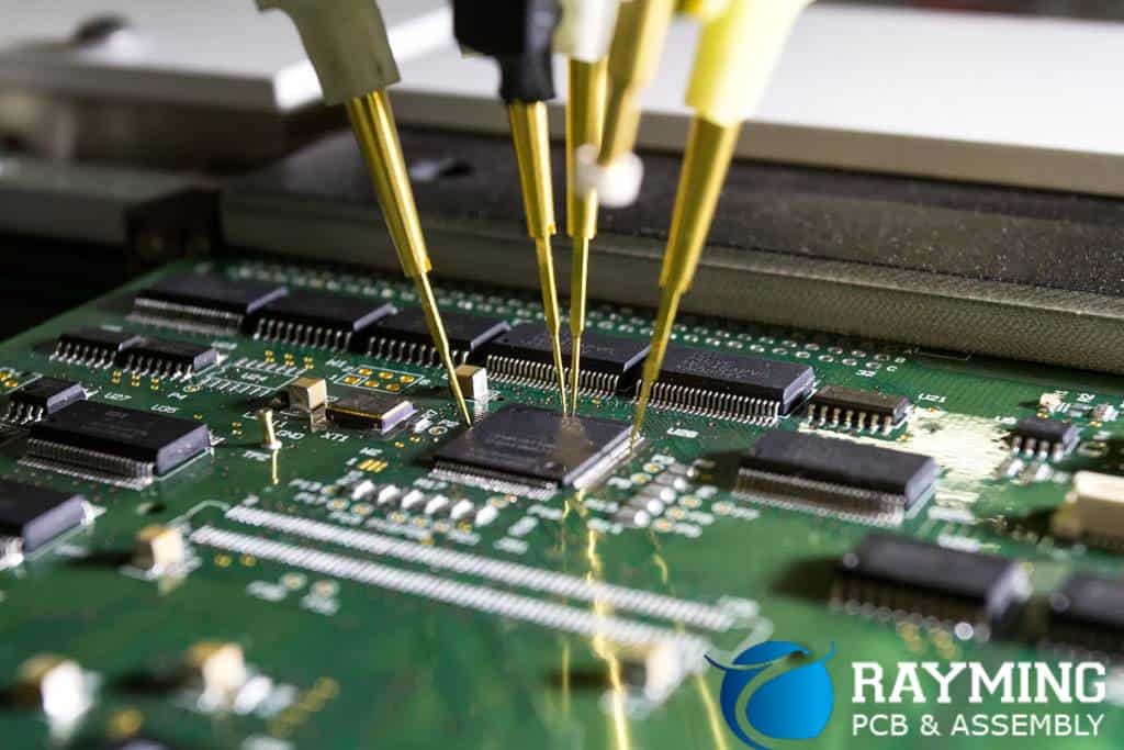
Inspecting SMT Assemblies
Verifying reliable construction of solder joints hidden underneath body packages requires several imaging techniques validating component attachments:
| Inspection Method | Description |
|---|---|
| Automated Optical (AOI) | 2D cameras rendering board images pinpoint misalignments against PCB CAD prints |
| X-Ray Imaging | Captures internal voids identifying insufficient joints under BGAs. Needs safety controls. |
| Sonic Scanning | High frequency sound waves reflect back spikes indicating gaps identifying cold joints under packages |
| Thermal Imaging | Scanning heat maps localize disconnected joints losing heat compared to surroundings |
| Cross-Sectioning | Physically cutting reveals joint shape and completeness inside the connection |
Multiple probing modes combine corroborating properly formed interconnects – critical for surface mount attachments concealed under devices.
Selecting SMT Assembly Processes
Determining appropriate surface mount production methods weighs optimal approaches matching speed, precision, automation factors, and volume considerations like:
| Process | Description | Volume Suitability |
|---|---|---|
| Robotic SMT Line | High throughput pick-place machines populate ~5000+ components per hour | Ten Thousand+ |
| Miniature SMT Line | Compact tabletop placement for small runs with 200 components per hour | Hundreds |
| Flex Printed Circuits | Conductive inks directly print simple circuits without component mounting | Very Low |
| Solder Paste and Reflow Oven | Manual paste screen printing and bench oven suits low volume complex boards | Few dozen |
| Soldering Iron | Hand soldering surface mount chips viable for prototypes or rework | Unit quantities |
Weighing tradeoffs between rate, flexibility, cost and complexity determines optimum processes for needs based on production maturity from research to mass manufacturing.
SMT Defects
Despite exacting controls, process deficiencies or component contingencies introducing anomalies must get identified inspecting assemblies with potential surface mount soldering failures shown here:
| Defect | Description |
|---|---|
| Cold Solder | Incomplete wetting from insufficient heat leaves right solidified blob with poor cohesion to pads risking detachment |
| Head-on-Pillow | Ball grid array outer balls reflow but interior joints blocked from flowing under body |
| Tombstoning | Released surface tension only grabs one end pitching parts vertically like tombstones instead of planar attachment |
| Blue Haze | White tin oxide plumes hinting moisture contamination interfering with reflow surface wetting |
| Solder Balls | Unintended solder droplets bridging pads or traces shorting electrically |
| Solder Bridging | Adjacent joint coalescence shorts pads electrically risking damage upon powering |
| Voids | Trapped bubbles within joints reduce effective thumbnail area degrading thermal capacity leading to thermal fatigue and potential cracking over life |
Catching flaws before boards ship ensures root causing assembly equipment or process adjustments vital for continuous improvement targeting defect-free SMT production.
Reworking SMT Assemblies
Remediating boards with soldering defects or requiring component replacements demands specialized SMT rework skills:
Soldering Irons – Fine contact thermal tips reflow/remove specific joints under microscope without disturbing neighboring solder. Preheater plates help.
Solder Wick – Fine braided copper strands soak up melted solder wicking it away clean from pads without damaging masks for resoldering
Hot Air Stations – Focused high temperature air streams locally heat joints loosening components from anchoring solder without affecting nearby parts.
Adhesives – Tiny resin deposits temporarily tack devices during rework awaiting finalized soldering avoiding movement
Stencils – Mini laser-cut solder paste applicators enable printable repairs to exactly where needed.
When failures occur post assembly, surgical SMT reworking skills rescue complex boards and avoid scrapping expensive PCBs due to localized defects.
Summary
SMT assembly established itself as the predominant electronics packaging and attachment technique as increasing component and product densities forced adoption from earlier through-hole methods unable to provide routing capabilities at minute scale. This overview covered key SMT facets:
- Component sizes ranging down dramatically
- Fine pitch terminations crowding underneath bodies
- Automation through accurate pick placement machinery
- Reflow processes soldering precisely formed joints
- Inspection methods targeting reliability
- Rework techniques enabling recovery
Appreciating these core SMT attributes in the context of printed circuit board developments that collectively enabled proliferation of today’s pervasive digital electronics provides perspective on this pivotal fabrication disruption ultimately reshaping electronics manufacturing.
Frequently Asked Questions
Here are answers to some common questions about SMT in the context of PCBs:
Can SMT soldering attach thru-hole components or connectors?
It becomes challenging since reflow oven conveyor processes differ considerably from wave solder equipment used for TH parts requiring wicking into barrels. Some through-hole pins splay out allowing partial SMT pad attachment.
What determines choosing component sizes like 0402 vs 0603 packages?
Smaller 0402 or 0201 chips save valuable board area but prove challenging handling or probing during development. Graduating towards 1206 or 0805 packages supports prototyping then back down for volume production.
Can solder mask fully encapsulate SMT landing pads or should copper be exposed?
The solder mask should at least have openings just larger than pads to allow paste application onto some exposed copper. Fully tenting risks failure if mask adhesive pulls off pads lifting traces.
Why are 0 ohm resistors occasionally seen on SMT boards?
Resistors convert jumper configurations into standardized SMT components allowing routing on inner layers to segregate signals groups. They act like zero-impact wires simplifying layouts through consistent practices.
How often do pioneered SMT production lines require recalibration or servicing?
Scheduled servicing adjusting nozzle tip alignments, replenishing consumables, cleaning and benchmarking calibration standards helps maintain equipment reaching rated precision targets consistently producing quality soldering year after year 24/7.


0 Comments