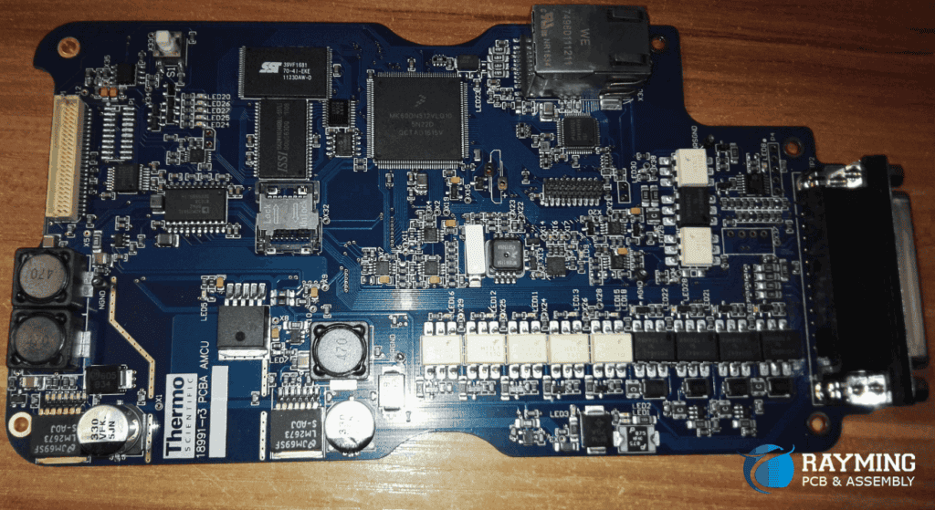
What is a PCBA Circuit Board?
A printed circuit board assembly (PCBA) is a populated printed circuit board (PCB) containing electronic components such as integrated circuits, resistors, capacitors, and connectors. The components are soldered onto the PCB to create a functional electronic circuit. PCBAs form the core of most electronic products including computers, mobile phones, automotive electronics, and consumer appliances.
PCBAs consist of:
- Bare PCB – The bare printed circuit board is made of a non-conductive substrate such as FR-4 with copper traces to route signals between components. The PCB provides the foundation to mount and connect electronic components.
- Components – Active and passive surface mount devices (SMD) or through-hole components that perform the electronic functions. Common components include integrated circuits (ICs), transistors, diodes, resistors, capacitors, inductors, and connectors.
- Solder joints – Solder electrically and mechanically connects component leads or terminals to the PCB pads and traces. Solder can be applied by wave soldering, reflow soldering, or manual soldering.
- Conformal coating – A thin polymeric coating applied over the PCBA for protection against moisture, dust, chemicals, and temperature extremes.
- Markings – Identifiers such as reference designators, polarity markings, and logos are screen printed on the PCB.
<img src=”/uctable.jpg”>
Fig 1. Exploded view of a typical printed circuit board assembly (PCBA)
PCBA Manufacturing Process
PCB assembly involves soldering surface mount (SMD) and through-hole (THT) components onto printed circuit boards using soldering equipment and various assembly processes. The typical steps are:
1. Printed Circuit Board Fabrication
- A bare PCB is fabricated based on the board layout design files. The PCB consists of a non-conductive substrate with copper traces, pads, vias, and plated through holes.
2. Solder Paste Screen Printing
- Solder paste is screen printed onto PCB pads through a metal stencil to provide adhesive and electrical contact.
3. SMD Placement
- SMD components are precisely placed onto the solder paste deposits on the PCB using automated pick and place machines.
4. Reflow Soldering
- The PCB passes through a reflow oven melting the solder paste to form reliable solder joints to anchor components.
5. Through-Hole Component Insertion
- Components with leads like connectors are inserted into plated through-holes either manually or automatically.
6. Wave Soldering
- The PCB passes over a molten wave of solder forming joints between TH components and PCB pads.
7. Cleaning
- Flux residues are cleaned from the soldered board using solvents.
8. Conformal Coating
- A protective coating may be applied over the assembled PCB.
9. Testing and Quality Inspection
- 100% electrical testing verifies all components were properly soldered with quality solder joints. Automated optical inspection looks for assembly defects.
10. Marking and Laser Engraving
- Reference designators, part numbers, logos, and texts can be screen printed or laser marked on the PCB.
This combination of automated assembly and selective manual assembly produces quality circuit boards efficiently. The process must be carefully optimized to ensure high yields with minimum defects.
Types of PCB Assemblies
There are several types of PCB assemblies used in electronics:
Single-sided Assembly
A single-sided PCB has components on only one side of the board. Less complex, low cost boards.
Double-sided Assembly
Components are mounted on both sides of the PCB. Allows greater component density.
Multi-layer Assembly
Components on outer layers with internal power and ground planes connected by plated through holes. Used for complex, compact boards.
Rigid PCB Assembly
The most common type using rigid FR-4 substrates. Low cost and widely supported by assembly equipment.
Flex PCB Assembly
Uses flexible polyimide substrates to interconnect other PCBs. Good for high flex applications. Requires special assembly processes.
Rigid-Flex PCB Assembly
Combines both rigid boards and flex circuits together into one assembly. Used to optimize routing and packaging.
HDI PCB Assembly
High density interconnect boards have tighter tolerances and trace spacing allowing greater component density. Used in compact products.
Metal Core PCB Assembly
Uses thermally conductive metal substrate to spread heat. Used in high power electronic products.
PCBA Design Considerations
The PCB design is a key factor determining the manufacturability, cost, and quality of the board assembly. Here are some key considerations:
Component Selection
- Choose component packages and pinouts supported by assembly processes. Avoid odd form factors when possible.
Component Placement
- Optimize placement for efficient automated assembly. Group components logically. Allow access for rework when needed.
Landing Pattern Design
- Use appropriate pad shapes, sizes, and spacing for different component packages and soldering processes.
Board Density
- Find the right balance between component density and manufacturability. Very dense boards are harder to assemble without defects.
Layer Stackup
- Use optimal number of layers to route traces effectively while minimizing layer count for cost. Allow space for power and ground planes.
Thermal Management
- Ensure components have access to thermal reliefs in pads and planes to dissipate heat. Add thermal vias if needed.
Test Points
- Include test points to probe signals and debug the board. Test pads should be safely located.
Board Outline and Edges
- Allow sufficient clearance between board edge and components. Avoid irregular board shapes. Radius corners to reduce stress.
Solder Mask Expansion
- Expand solder mask openings slightly past pads to account for registration tolerances during manufacturing.
Silkscreen Markings
- Add reference designators, polarity markings, and board information to aid assembly and troubleshooting.
With careful board design and component selection, PCB assemblies can be optimized for manufacturability, reliability, and cost effectiveness.
Benefits of Using a Contract Manufacturer
Many companies outsource PCBA production to contract manufacturers (CMs) that specialize in board assembly. The benefits include:
- Expertise – CMs have the technical expertise, assembly equipment, and processes to build quality boards. They keep up with the latest technologies.
- Scalability – CMs can scale production capacity up and down flexibly based on demand. No need to invest in fixed assets.
- Supply Chain – CMs manage the complex electronics supply chain including procurement, warehousing, and logistics.
- Quality – CMs have quality systems and processes to catch defects early. ISO certified facilities are available.
- Global Production – CMs have facilities around the world allowing production localization close to target markets.
- Cost Savings – By leveraging economies of scale, CMs can offer competitive pricing compared to in-house assembly.
- Fast Ramp Up – CMs can rapidly ramp up existing designs into volume production avoiding delays.
- One-Stop Service – CMs can provide turnkey services including PCB fabrication, component sourcing, assembly, testing, and even enclosure manufacturing.
Using an experienced, capable contract manufacturer allows companies to get quality assembled boards faster and more affordably.<img src=”/pcbgraph.svg”>
Fig 2. Contract manufacturers offer expertise, capacity, quality, and cost savings.
Key Factors When Selecting a PCBA Supplier
Here are key factors to evaluate when selecting a contract manufacturer for your PCB assembly needs:
- Technical Capabilities – Evaluate their experience with the assembly technology required for your boards such as SMT, through-hole, BGAs, microBGAs, flex/rigid flex.
- Quality Systems – Look for ISO certification, solder certification, quality processes, defect rates, repair capabilities. Conduct audits.
- Supply Chain Management – Assess their component sourcing, inventory, logistics, and distribution capabilities.
- Geographic Locations – Determine if they have manufacturing sites in your target markets for regional production.
- Certifications – Check if they meet regulatory or industry specific compliance certifications needed.
- Engineering Support – Evaluate their design, prototyping, NPI, and volume production engineering capabilities.
- Production Capacity – Do they have sufficient capacity and flexibility to meet your volume needs now and in the future?
- Customer Service – Gauge responsiveness to quote requests, change orders, technical queries. Check references.
- Cost – Compare assembly pricing models (turnkey, consigned, etc) and total landed costs. Understand tradeoffs.
By thoroughly evaluating CMs on these key factors, you can select reliable partners for your PCBA needs and ensure successful outsourced assembly.
Conclusion
Printed circuit board assembly is a complex, specialized manufacturing process requiring expertise and precision equipment to populate electronics boards with components accurately and efficiently. Well designed PCBs and optimal assembly processes result in quality boards with maximum yields. Partnering with a capable, experienced contract manufacturer provides access to advanced manufacturing capabilities and enables companies to ramp up and scale production of innovative electronic products faster and more affordably.
Frequently Asked Questions
What are the most common defects in PCB assembly?
Some of the most common PCBA defects are:
- Solder bridges – Unintended solder connections between pads or traces causing shorts.
- Solder voids – Insufficient solder fill in a joint reducing strength.
- Poor solder joints – Weak looking, dull, or cracked solder joints with high resistance.
- Wrong components – Incorrect component values or types assembled on the board.
- Misaligned components – Component placement outside normal tolerances leading to skew.
- Missing components – Components entirely left off the board.
- Damaged PCBs – Cracks, nicks, handling damage, or drill smear on PCBs.
- Excessive solder – Solder globs, spikes, flags, or splashes.
What is the difference between SMT and through hole assembly?
SMT or surface mount technology uses smaller components with leadless contacts that mount directly to the surface of the PCB. TH or through hole components use cylindrical or axial leads that insert into holes in the PCB. SMT improves density and process automation while TH provides strength for connectors. Many boards use both SMT and TH assembly.
How are components held in place before soldering?
SMD components are held in place by solder paste prior to reflow soldering. The solder paste is tacky and provides adhesion to the PCB pads to fix components. For through hole components, the leads inserted in holes mechanically retain components before wave soldering. Glue is sometimes used for additional retention when needed.
What is an open circuit defect in a PCBA?
An open circuit means an unintended break in electrical conductivity in a PCB trace or solder joint so current cannot flow. Some causes are damaged traces, cold solder joints, solder voids, component lead breakage, or loose connectors. This can prevent circuit board operation.
How can you prevent electrostatic discharge damage in PCB assembly?
ESD prevention techniques:
- Use ESD safe materials: antistatic plastic bags, ESD flooring.
- Ensure constant wrist straps grounding of assembly technicians.
- Use ionization bars to neutralize static charge buildup.
- Keep humidity between 40-60% to reduce static electricity.
- Use ESD protective packaging for PCB transport and storage.
ESD control is critical to avoid damaging sensitive components during PCBA handling.


0 Comments