Printed circuit boards (PCBs) are an integral part of most electronic devices and equipment. Understanding the PCB manufacturing process is important for engineers and product developers looking to produce high-quality and reliable circuit boards. This comprehensive guide provides a step-by-step overview of the PCB fabrication process, from designing the board layout to shipping the finished boards.
PCB Design And Layout
Schematic Capture
The first step in the PCB manufacturing process is schematic capture. This involves using EDA (electronic design automation) software to draw a schematic diagram showing the logical connections between electronic components. Symbols represent the actual electronic devices and lines connecting them indicate electrical connectivity.
At this stage, the engineer focuses solely on representing the circuit logically while the physical layouts of components are defined in the next steps.
PCB Layout
After completing the schematic diagram, the PCB layout is created. This stage defines the exact physical footprint of the circuit on the printed circuit board.
Here the components in the schematic are virtually placed on a PCB grid canvas and the interconnectivity is defined by drawing copper tracks. The layout software allows for placement constraints, routing connections automatically, and design rule checks.
Key aspects considered at this stage:
- Component placement for optimal signal trace routing
- Board dimensions, layer stackup
- High-speed routing, impedance control
- Accommodating connectors, peripherals
Generate Manufacturing Files
Once the PCB layout is finalized, the data must be converted into files used to manufacture the board.
Common file formats for PCB fabrication include:
- Gerber files: Contains image data of copper layers, solder mask, silkscreen, etc.
- Drill files: Specifies hole sizes and locations
- BOM: Lists all materials and components for assembly
- Netlist, centroid, and position files
The files are then sent to the PCB manufacturer for prototyping or volume production.
PCB Prototyping vs Production
PCB prototyping involves manufacturing a small number of boards (usually ≤10) to validate the design before large-scale production. This allows testing the board’s fit and functions early in the development process.
Once the prototype has been proven, design optimizations are incorporated, and testing is completed, volume production starts. This manufactures boards at larger economies of scale to be installed in actual products.
| Parameter | Prototype | Production |
|---|---|---|
| Quantity | 1-10 boards | Hundreds to thousands |
| Lead Time | 24 hours to 4 weeks | 4-8 weeks |
| Testing | Extensive testing done | Limited testing |
| Cost | High per board | $2-10 per board |
| Process | Same as production | Highly automated |
PCB Fabrication Process Technologies
Modern PCB fabrication relies on the following key technologies:
Subtractive Processes
This method starts with a copper-clad laminate board and then etches away (subtracts) unwanted copper to leave the desired copper traces behind.
Steps:
- Start with glass reinforced epoxy laminate sheet fully coated with copper on one or both sides
- Apply photoresist coating on copper surfaces
- Expose photoresist to UV through a film printed with the PCB pattern mask.
- Develop the photoresist to remove exposed areas, leaving behind a pattern matching the desired copper traces
- Etch away copper from areas unprotected by photoresist
- Strip off remaining photoresist to reveal finished PCB copper pattern
This technique can produce fine 8 mil lines and spaces. However, it generates hazardous chemical waste.
Additive Processes
Rather than etching away copper, this technique builds up the pattern by adding copper only where needed.
Steps:
- Start with bare glass reinforced epoxy laminate
- Catalyze board surface to accept copper electroplating
- Mask areas that should remain copper-free
- Electroplate entire board surface with thin copper layer
- Strip off mask to leave behind desired copper pattern
Additive processing produces very fine 6 mil lines without etching. But it requires managing the electroplating bath.
Semi-Additive Process
This combines aspects of subtractive and additive methods.
Steps:
- Start with fully copper-clad laminate
- Apply photoresist except on areas needing tracks
- Electroplate copper on unmasked areas to desired thickness
- Strip off photoresist
- Etch away original thin copper leaving thicker plated tracks
The semi-additive approach is most common today due to lower costs and high circuit density.
Laser Photo Ablation
Rather than chemicals, this process uses laser beams to selectively remove copper cladding.
Steps:
- Start with copper-clad dielectric board
- Cover board with mask material opaque to laser wavelength
- Expose desired copper areas by scanning focused laser
- Remove evaporated mask and debris to reveal finished tracks
This eliminates waste and chemicals, but involves high equipment costs.
Printed Electronics
An emerging PCB fabrication technique uses inkjet printing technology to directly print conductive ink onto the substrate.
Steps:
- Design circuit layout
- Load substrate (glass, PET, fabric, etc) on print bed
- Inkjet print silver nanoparticle ink to form tracks
- Thermal cure inks
- Repeat layering to achieve multi-layer circuit
Printed electronics enables rapid prototyping, design flexibility and embedded electronics.
Key Steps In PCB Fabrication Process
Now let’s go through the typical PCB manufacturing process steps used in volume production:
1. Substrate Material Cutting
The process starts with bare FR-4 or CEM substrate sheets comprising woven fiberglass and epoxy resin. Sheets are cut down to the required PCB panel sizes either manually or using a laser/mechanical cutting machine.
PCB Substrate Sheet Cutting
Factors considered:
- Panel dimensions dictated by product PCB size
- Number of boards per panel to optimize material utilization
- Tooling holes added for material handling
- Allowance for trim and break tab regions
2. Through Hole Drilling
For boards with through hole components, this step first drills holes at locations matching the position file.
A CNC mechanical drill machine is used with different drill bits to produce holes ranging from 0.3mm to 6mm in diameter typically.
The position accuracy achieved is within 0.1mm while achieving excellent hole perpendicularity.
3. Surface Polish
Boards then undergo abrasive planarization to remove drill smear and debris left behind. This renders a flat uniform surface needed for subsequent photolithography.
Rotary brush polishing is commonly employed, along with coarse to fine abrasives. This leaves behind a smooth copper surface ready for coating.
4. Apply Photoresist
The core of PCB fabrication relies on photolithography to selectively form the copper pattern on insulating substrate. This requires coating the substrate with photosensitive material that hardens when exposed to specific light wavelengths.
Liquid or dry film photoresist is applied covering the entire copper surface through automated rollers. This photoresist layer must have uniform thickness and be free of bubbles or dust particles.
Applying Liquid Photoresist on PCB
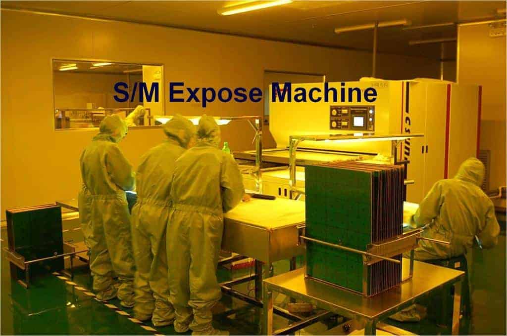
5. Exposure Through Artwork Film
Next, the photoresist coating must be selectively exposed to match the desired circuit pattern. This is achieved using litho sheets or artwork film printed with the layout design placed directly over the PCB panel photoresist surface.
The setup then undergoes a blanket UV exposure flood. The opaque areas of the litho sheet block UV reaching photoresist underneath. But UV passes through transparent regions hardening the coating below.
6. Developing Away Unexposed Resist
The panel goes through a developing solution bath which washes away any uncured photoresist left unexposed previously.
This leaves behind cured photoresist only in the desired PCB track pattern. Copper areas needing to be etched away are now revealed underneath.
7. Etch Copper
The PCB then undergoes etching where copper unprotected by photoresist gets dissolved away into the etchant solution.
Common etchants used include:
- Ammonium Persulfate – Most common for copper substrate
- Ferric Chloride – Higher copper compatibility
- Hydrogen Peroxide-Sulphuric Acid – For both copper and tin substrates
Etchant agitation, concentration and temperature are controlled to achieve a 0.1 mil etching precision.
8. Resist Strip
The panels are immersed in a caustic stripping solution dissolving away all the remaining cured photoresist masking material used until now.
This reveals the finished copper traces patterned on the uncovered board substrate according to the original circuit layout.
9. Surface Finish Electroplating
To protect copper tracks from corrosion and improve soldering compatibility, metallic surface finishes are applied atop the conductors.
Common finishes electroplated include:
- Hasl (Tin-Lead): Most economical finish. Creates leaded solder coating.
- Immersion Tin: Excellent for soldering. Resists oxidation/tarnishing.
- Immersion Silver: Lowest contact resistance. Compatible with wire bonding.
- OSP (Organic Solderability Preservatives): Organic coating to enable soldering. Low cost.
- ENIG (Electroless Nickel Immersion Gold): For highest performance/reliability applications. Expensive.
The board panel serves as the cathode while metallic ions from the electroplating solution deposit onto exposed conductors giving the desired solderable finish.
10. Soldermask Lamination
The panel then gets covered by a green solder masking material wherever conductors should be protected from solder bridges or external contacts. This is achieved by laminating dry film or applying liquid photoimageable soldermask and curing.
Openings are created in the soldermask coating through selective light exposure and developing to reveal pads needing soldering or connectors.
11. Silkscreen Printing
Legends and identifiers are printed onto the PCB using epoxy-based ink through the silkscreen process. This creates a permanent white marking resistant to handling, scratches and solvents.
The ink is squeegeed through a stainless steel mesh stretched over a pattern matching the board overlay graphics. This ink cures at high temperatures.
12. Surface Finish
A protective coating is additionally applied through dipping or spraying onto exposed copper traces. This guards against corrosion or handling damage during assembly or operation.
Common final finishes include:
- Immersion silver: Prevents copper oxidation
- Immersion Tin: Resists tarnishing. Compatible with silver, gold and palladium surfaces.
- Conformal coating: Insulating polymer layers like acrylic, silicone, and urethane. Help insulate against particles or moisture ingress.
- ENEPIG (Electroless Nickel Electroless Palladium Immersion Gold): Maximum reliability in harsh environments. Costs higher.
13. Electrical Testing
Once board fabrication completes, testing starts by checking electrical connectivity and isolation across all nets using fixture probes. Continuity between connected nodes and absence of shorts between isolated nets verifies PCB integrity.
This validates the fabrication process has correctly realized the intended physical connectivity encoded within the digital layout data. Automated Optical and X-ray inspection can supplement electrical testing.
14. Panel Singulation
The finished PCB panel consisting of multiple unit boards in laid out in an array now undergoes singulation into individual boards. Hard tooling and fixtures ensure dimensional accuracy during depanelization.
Techniques employed include routing, scoring or v-cutting. Clean breaks are made possible by leaving small uncut tabs intact within the openings.
15. Quality Inspection
Prior to shipment, boards undergo a thorough quality inspection assessing parameters like:
- Line width and spacing
- Hole position/size
- Pad dimensions
- Copper thickness
- Surface finish conformity
Optical cameras aided by image processing check for defects while custom fixturing allows capturing images systematically across the entire board area.
This allows identifying any fabrication faults needing correction or scope for process improvements in future production runs.
16. Packaging and Shipment
Once cleared for quality, boards get packed with proper labeling into ESD-safe boxes, tubes or cut-paneled racks. Environmental conditions must be maintained even in transit to avoid moisture absorption or oxidation before assembly.
Shipment is via road or air transport providers to the OEM facility for component population.
Key PCB Technology Advancements
PCB technology has rapidly advanced enabling high-density multi-layer boards with fine geometries to power modern electronics. Some significant upcoming developments include:
5G Antennas Embedding: Embedding antenna elements and RF signal traces within the board layers enables compact high-frequency circuit and antenna integration.
Aluminum Substrate: Thermal mapping can customize back-drilling algorithms adapting to dynamic thermal gradients to achieve 10x better heat dissipation using aluminum boards.
Flexible Boards: Foldable circuits interconnect discreet rigid islands allowing flexible stretchable conduits achieving durability with 28um ultra-thin polyimide substrates.
Embedded Passives: Printed and laser trimmed resistors or capacitors integrated into the PCB layers eliminates discrete passives components dramatically saving space.
Microvias in Pad: Reduces layer transition via sizes down to 25um allowing pad area recovery achieving 40% improved routing density even for 20+ layer complex boards.
Direct Metallization: Avoids photoresist processing by directly ablating substrate with picosecond laser pulses to vaporize material pixels matching copper pattern design.
Sequential Buildup: Fabricating inner layers and outer layers in separate lines improves production economics when higher layer counts are required only for advanced packaging techniques.
PCB Design Guidelines
Following PCB design guidelines facilitate fabrication, quality and reliability:
1. Match Line Widths And Spaces To Capabilities
Route tracks based on manufacturer’s offered trace/space rules for optimal yield. Finer geometries cost more.
2. Incorporate Test Points And Fiducials
Include pads connected to nets for probing during fabrication/assembly testing. Fiducials assist machine imaging.
3. Follow Conductor Current Density Limits
Use suitable widths to avoid overheating risk under maximum load. W = K/ΔT where K is conductor thermal property.
4. Control Impedance Of High-Speed Traces
Match characteristic impedance Zo to source/load for good signal integrity. Zo is determined by W, H (trace thickness, height over ground plane).
5. Ensure Adequate Board Rigidity
Avoid excessive warpage through central cores/stiffeners, copper fills and minimum 3 mil trace/space on outer layers.
6. Check Component Placement Densities
Distribute parts evenly between layers. Watch for congested zones exceeding 30 components per square inch.
7. Include Board Handling Fixtures
Incorporate mouse bites, positioning holes, conveyor rails etc. needed for material handling during fabrication and assembly.
8. Minimize Sensitive Crossovers
Reduce analog to digital crossovers. Use tighter clearances, avoid T-junctions.
9. Define Copper Pullbacks For Closely-Spaced Components
Ensure clearance from pad allowing rework for tight component pitch nearing 13 mils (0.33mm).
10. Split Ground Planes Below Closely-Spaced Devices
Isolate analog/digital return paths. Minimizes current loop noise pick up by sensitive low-level analog components.
Frequently Asked Questions
Here are some common queries regarding the PCB manufacturing process:
Q1. How accurate are drill hole positions and hole sizes?
Mechanical drilling can achieve positional accuracy within 0.1mm and hole size tolerance down to +/- 0.05mm. For higher precision demands, laser drilling offers accuracy levels reaching down to +/- 0.025mm.
Q2. How are very fine 8 mil line width and spacing achieved?
This relies on advanced photoresists, using dry film laminates, vacuum contact between the mask-board sandwich and high intensity collimated UV exposure in yellow light. Semi-additive plating can also attain 6 mil geometries.
Q3. What surface finishes allow wire bonding application?
Immersion silver with 30 micro-inches thickness enables very low contact resistance for ultrasonic or thermosonic wire bonding interconnections. Flash gold plating over nickel underlayer also offers wire bonding capability.
Q4. How is impedance controlled for routing high-speed signals?
Maintaining target impedance Zo requires managing trace geometry and dielectric material properties. Wider lines spaced further from their reference plane lowers Zo. Narrower lines with thinner dielectrics raises Zo.
Q5. Why are mouse bites and fiducials necessary?
Mouse bites assist with properly fixturing panels together or breaking apart individual boards from the main panel by inserting pins in the holes during depanelization. Fiducials guide imaging systems to orient the board correctly during optical inspection.
Conclusion
Understanding the end-to-end PCB manufacturing process empowers designers to make prudent layout decisions and helps manufacturers contingency plan to assure product delivery timelines.
Continued advancements in fabrication technology widens the possibilities for denser multi-layered boards able to meet the needs of sophisticated electronics applications – from smartphones to autonomous electric vehicles to data centers and more.


0 Comments