
What is PCB layout structure?
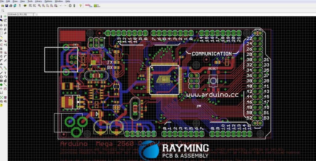
Printed circuit board (PCB) layout is the design of traces, pads, and other conductive features that connect different components on a PCB. The layout establishes the component positions and interconnections for an electronic circuit. Proper PCB layout is crucial for a functioning, noise-free PCB with signals routed clearly between components.
Key Design Rules and Principles
When laying out a PCB, engineers must follow certain design rules and principles:
Component Placement
Appropriate component placement establishes efficient routing with short traces and clear connectivity between related sections. Guidelines include:
- Group associated components together
- Place high-speed components close together
- Separate analog and digital sections
- Position heat-sensitive parts away from heat sources
Routing
Trace routing connects pads following best practices:
- Use 45° and 90° angles rather than curves
- Route traces on one layer at a time whenever possible
- Use wider traces for higher current
- Avoid crossing split ground planes with traces
Signal Integrity
Maintaining signal integrity keeps signals clear and noise-free:
- Match trace widths to signals
- Minimize vias and stubs
- Use ground and power planes to isolate signals
- Include decoupling capacitors near IC power pins
Manufacturability
Design for manufacturability eases PCB fabrication and assembly:
- Allow adequate clearance between traces and pads
- Make pad sizes appropriate for hole drilling
- Follow minimum trace width and spacing rules
- Allow room for vias and test points
Sections of a PCB Layout
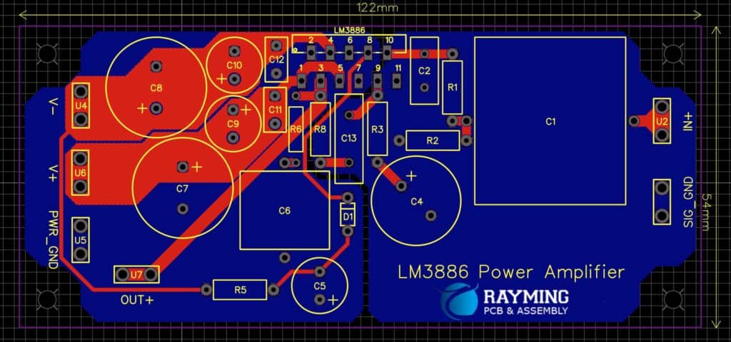
A typical PCB layout contains several key sections:
Power Supply
The power supply provides necessary voltages and currents to components. Good power distribution and decoupling helps reduce noise. The power supply section includes:
- Power and ground planes
- Regulators and conversions chips
- Bulk and bypass capacitors
- Power connectors or pads
Processor and Memory
The processor executes program instructions while memory chips store code and data. This section links the processor to memories and peripherals:
- Microcontroller or microprocessor IC
- Support circuitry like crystals and supervisory chips
- RAM, ROM, Flash and other memory ICs
- Address, data and control signals
Analog Circuitry
Analog circuits interface sensors, condition signals, control outputs and perform other continuous functions:
- Ampilifiers, filters and analog-based ICs
- Sensitive traces matched to signals
- Often separated from digital sections
- May include shielding or ground planes between analog signals
Digital Circuits
Digital logic provides discrete on/off signals for computations, timing control and decision-making:
- CPLDs, FPGAs, shift registers, multiplexers
- Short connections to avoid noise and interference
- May connect to processor bus signals
RF Modules
Wireless PCBs include dedicated RF sections with coaxial interconnects and impedance-controlled transmission lines:
- Antennas, oscillators, mixers
- Shielding partitions to contain interference
- Impedance-matched traces, transmission lines and pads
Connectors
Connectors allow interfacing between a PCB and other circuits or external components:
- Edge card connectors
- Coaxial connectors for RF signals
- Board-to-wire connectors
- Headers and receptacles
Layout Challenges and Solutions
PCB layout involves navigating design challenges including:
Cross-Talk
Cross-talk occurs when closely spaced traces couple noise onto adjacent signals. Solutions include:
- Increase spacing between traces
- Route signals on separate board layers
- Insert ground traces or copper pours between signals
| Type | Description | Mitigation Techniques |
|---|---|---|
| Capacitive Coupling | Electric field interactions between adjacent traces | – Wider trace spacing<br>- Ground planes blocking fields |
| Inductive Coupling | Magnetic field interactions cause noise pickup | – Avoid parallel traces<br>- Cross at 90° angles |
Impedance Control
Impedance mismatches reflect signals and distort data transmission:
- Use impedance-matched traces, pads, vias for high-speed signals
- Calculate required trace widths and distances for target impedance
- Controlled-impedance design rules in layout tools
EMI/RFI Interference
Stray electromagnetic interference (EMI) disrupts sensitive components. Solutions include:
- Enclose circuitry in shielded compartments
- Isolate analog/RF routing from digital traces
- Include ground and power planes to absorb EMI
- Use bandpass filters, ferrite beads to suppress noise
Thermal Management
Excessive heat impacts performance and longevity. Effective thermal techniques:
- Position heat-sensitive ICs away from heat sources
- Include thermal pads/vias to conduct heat to ground planes
- Use thicker copper weights on inner board layers
- Add cutouts on the board to facilitate airflow
FinalVerification
Verification validates the layout before manufacturing PCB prototypes:
- Design rule checks confirm trace spacing/widths meet specifications
- Electrical rule checks locate shorts, opens and other errors
- Signal integrity analysis through simulation spot glitches
- Review layout visually checking placement, rotation and footprints
Catching issues early avoids costly re-spins further into the development process. Common checks performed during layout verification include:
| Type | Check | Problem |
|---|---|---|
| Design Rules | Trace width/spacing | Undersized traces overheat |
| Electrical Rules | Short circuits | Damage, fires |
| Open traces | Intermittent faults | |
| Signal Integrity | Transmission line effects | Signal distortion |
| Visual Checks | Component placement | Wrong orientation won’t function |
| Footprint correctness | Wrong pads break connectivity |
FAQ
What are the most important parts of the board to layout first?
Focus first on the power supply, decoupling capacitors and other power distribution components since these establish the foundation supplying currents and voltages to all sections of the circuitry. Next prioritize high-speed components like the processor and memories which pass signals between many parts of the system.
What are common PCB layer stackups?
A typical 4-layer board stackup is:
- Top: Signals
- Layer 2: Ground
- Layer 3: Power
- Bottom: Signals
Additional layers may include more signal routing layers, shielding ground planes, embedded passive layers with capacitance for decoupling, and thicker copper cores to dissipate heat.
How close can two traces be routed next to each other?
The minimum clearance between traces depends on PCB fabrication limitations and isolation requirements. Standard design rules often specify 4-10 mil spacing between same-layer traces. Closer routing risks shorting while wider gaps take up board area.
What is the best software for designing PCB layouts?
Popular PCB layout software packages include Altium Designer, Cadence Allegro, Mentor Graphics Xpedition, and Zuken CR-8000. Many engineers use Altium for its cost-effectiveness, extensive component libraries suited for complex designs, and multiple analysis tools to verify layouts.
How long does it take to layout a typical PCB design?
Layout time varies substantially depending on the design complexity, component density, routing difficulties, number of layers, and engineer skill/experience. Simple designs may require just a few days while complex RF, high-speed-digital, or dense boards often take four to six weeks with multiple engineers working together.