Printed Circuit Board (PCB) design is a crucial process in the development of electronic devices, ranging from simple consumer electronics to complex industrial systems. PCBs act as the backbone of electronic circuits, providing a platform for mounting and interconnecting electronic components. Designing a PCB involves various stages, each requiring meticulous attention to detail and adherence to industry standards and best practices. In this comprehensive article, we will explore the steps involved in PCB designing, from concept to final production.
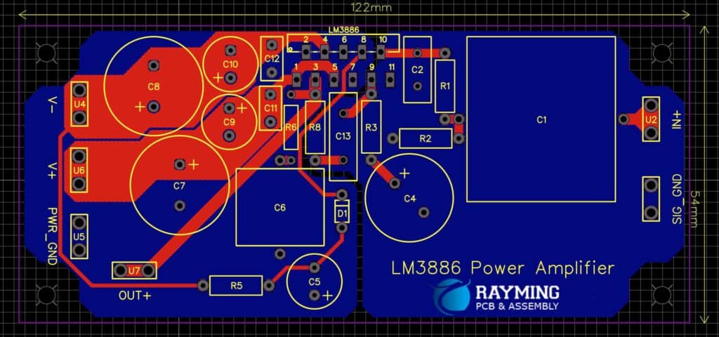
Table of Contents
- Understanding the Design Requirements
- Schematic Capture
- Component Selection and Footprint Assignment
- PCB Layout
- 4.1 Component Placement
- 4.2 Routing and Trace Design
- 4.3 Power and Ground Planes
- 4.4 Design Rule Checking (DRC)
- PCB Manufacturing Data Preparation
- Prototyping and Testing
- Design Verification and Validation
- Design Finalization and Documentation
- Frequently Asked Questions (FAQs)
Understanding the Design Requirements
The first step in PCB designing is to thoroughly understand the design requirements. This involves gathering information about the project’s specifications, functional requirements, environmental constraints, and any applicable industry standards or regulations. Some key considerations at this stage include:
- Functional requirements: Identify the specific functions and features the PCB must support, such as digital signal processing, analog circuits, power management, or communication interfaces.
- Performance requirements: Determine the necessary performance criteria, such as operating frequencies, signal integrity, power consumption, and thermal management.
- Environmental requirements: Consider the operating conditions, such as temperature ranges, humidity levels, and any potential exposure to vibrations, shocks, or electromagnetic interference (EMI).
- Size and form factor constraints: Understand the physical dimensions and space limitations for the PCB design.
- Cost and production requirements: Evaluate the target production volume, cost targets, and any specific manufacturing techniques or materials required.
Thorough understanding and documentation of these requirements are essential for ensuring a successful PCB design that meets the project’s objectives.
Schematic Capture
Once the design requirements are well-defined, the next step is to create the schematic diagram. The schematic is a graphical representation of the electronic circuit, showing the interconnections between various components and their logical relationships.
During schematic capture, engineers use electronic design automation (EDA) software tools to create the circuit diagram. This process involves the following tasks:
- Component selection: Choose the appropriate electronic components, such as integrated circuits (ICs), resistors, capacitors, and connectors, based on the design requirements and specifications.
- Circuit design: Arrange the components on the schematic canvas and establish the connections between them, representing the desired circuit functionality.
- Electrical rules checking (ERC): Perform ERC to identify and resolve any potential electrical errors, such as short circuits, open connections, or incorrect component values.
- Annotation: Assign reference designators and other identifiers to components for easier navigation and documentation.
- Simulation (optional): Conduct circuit simulations to verify the expected behavior and functionality of the design before committing to PCB layout.
The schematic capture stage is crucial as it serves as the blueprint for the subsequent PCB layout process and ensures that the final design meets the intended circuit functionality.
Component Selection and Footprint Assignment
After completing the schematic capture, the next step is to select the appropriate physical components and assign their corresponding footprints (land patterns) on the PCB. Footprints define the physical dimensions and pad layouts required for mounting components on the PCB surface.
This stage involves the following tasks:
- Component selection: Choose the specific components from available manufacturers, considering factors such as package types, operating characteristics, and availability.
- Footprint assignment: Assign the correct footprint for each component based on its package type and manufacturer specifications.
- Footprint validation: Ensure that the assigned footprints comply with the design rules and manufacturing capabilities of the intended PCB fabrication process.
- Component placement constraints: Define any specific placement constraints or keep-out regions for certain components, such as maintaining minimum clearances or avoiding sensitive areas.
Accurate component selection and footprint assignment are crucial for ensuring proper component mounting, electrical connectivity, and adherence to design rules during the PCB layout stage.
PCB Layout
The PCB layout stage is the heart of the PCB design process, where the physical arrangement of components and interconnections are defined on the PCB surface. This stage involves several critical tasks:
Component Placement
Component placement involves strategically positioning the components on the PCB surface while considering various factors, including:
- Signal routing optimization: Arrange components to minimize trace lengths and reduce signal interference.
- Thermal management: Position high-power components in areas with efficient heat dissipation or near thermal vias.
- Mechanical constraints: Ensure proper clearances for connectors, mounting holes, and other mechanical requirements.
- Design for manufacturability: Follow guidelines for component spacing, orientation, and placement to facilitate efficient assembly processes.
Effective component placement optimizes signal integrity, thermal performance, and manufacturability while also considering aesthetic considerations and design constraints.
Routing and Trace Design
Routing involves creating the physical interconnections (traces) between components on the PCB layers. This process involves several critical tasks:
- Trace width and spacing: Determine appropriate trace widths and clearances based on current-carrying requirements, signal frequencies, and manufacturing capabilities.
- Signal routing: Route critical signals with optimal trace lengths, minimizing vias (layer transitions), and avoiding high-noise areas or sensitive components.
- Differential pair routing: For high-speed or differential signals, ensure precise routing and matched lengths between pairs to maintain signal integrity.
- Impedance control: Maintain controlled impedance on high-speed signals by adjusting trace widths, clearances, and stack-up configurations.
- Crosstalk and EMI mitigation: Implement strategies such as ground planes, guard traces, and shielding to minimize crosstalk and electromagnetic interference (EMI) issues.
Careful routing and trace design are essential for ensuring signal integrity, power distribution, and electromagnetic compatibility (EMC) compliance.
Power and Ground Planes
Power and ground planes are solid copper layers within the PCB stack-up that distribute power and ground connections across the board. These planes serve several purposes:
- Power distribution: Provide low-impedance paths for power distribution, minimizing voltage drops and ensuring clean power delivery to components.
- Ground referencing: Establish a stable ground reference for signals, reducing ground loops and noise issues.
- Shielding and EMI reduction: Act as a shield against electromagnetic interference (EMI) and reduce radiated emissions.
Proper design and implementation of power and ground planes are critical for ensuring stable power delivery, noise reduction, and EMC compliance.
Design Rule Checking (DRC)
Design Rule Checking (DRC) is an automated process that verifies the PCB layout against a set of predefined design rules and manufacturing constraints. DRC ensures that the layout adheres to the specified requirements, such as:
- Trace width and spacing requirements
- Clearances between copper features and components
- Via sizing and placement rules
- Pad and hole size constraints
- Solder mask and silkscreen clearances
- Manufacturability checks (e.g., minimum annular ring, aspect ratios)
Performing DRC at various stages of the layout process helps identify and resolve potential issues before proceeding to the next step, reducing the risk of costly design iterations or manufacturing failures.
PCB Manufacturing Data Preparation
Once the PCB layout is complete and has passed the necessary design rule checks, the next step is to prepare the manufacturing data for PCB fabrication and assembly. This process involves the following tasks:
- Gerber file generation: Create Gerber files, which are standardized file formats that contain the necessary information for PCB fabrication, including copper layers, solder mask, silkscreen, and drill files.
- Assembly data preparation: Generate assembly data files, such as pick-and-place files, centroid data, and bill of materials (BOM), required for the automated assembly process.
- Documentation and notes: Prepare any additional documentation, assembly notes, or special instructions for the PCB manufacturer and assembly house.
- Design review and verification: Conduct a final design review and verification to ensure the completeness and accuracy of the manufacturing data.
Proper preparation of manufacturing data is crucial for ensuring accurate and reliable PCB fabrication and assembly, minimizing the risk of errors or defects.
Prototyping and Testing
Before committing to full-scale production, it is essential to create prototypes and conduct thorough testing to validate the PCB design. This stage involves the following tasks:
- PCB prototyping: Fabricate a small number of PCB prototypes using the manufacturing data generated in the previous step.
- Assembly and inspection: Assemble the prototype boards, ensuring proper component placement, soldering quality, and overall board integrity.
- Functional testing: Perform comprehensive functional testing of the assembled prototypes, verifying that the design meets the intended specifications and requirements.
- Environmental and reliability testing: Subject the prototypes to various environmental conditions (e.g., temperature, humidity, vibration) and conduct reliability tests to ensure the design’s robustness and durability.
- Design iterations: Based on the test results, identify and address any issues or design flaws by iterating on the design, if necessary.
Prototyping and testing are critical steps in the PCB design process, as they provide an opportunity to identify and resolve potential issues before committing to full-scale production, reducing the risk of costly recalls or field failures.
Design Verification and Validation
Throughout the PCB design process, it is essential to conduct thorough design verification and validation to ensure the design meets the specified requirements and adheres to industry standards and best practices. This stage involves the following tasks:
- Design reviews: Conduct regular design reviews with cross-functional teams, including electrical engineers, mechanical engineers, and manufacturing experts, to identify and address potential issues or design flaws.
- Simulation and analysis: Perform simulations and analysis, such as signal integrity analysis, thermal analysis, and electromagnetic compatibility (EMC) analysis, to verify the design’s performance and compliance with relevant standards.
- Compliance testing: Conduct compliance testing, such as EMC testing, safety testing, and environmental testing, to ensure the design meets applicable regulatory requirements and industry standards.
- Documentation and traceability: Maintain comprehensive documentation and ensure traceability of design decisions, changes, and revisions, enabling effective design control and version management.
Design verification and validation are ongoing processes that span the entire PCB design cycle, ensuring that the final product meets the intended specifications, performs reliably, and complies with relevant standards and regulations.
Design Finalization and Documentation
Once the PCB design has been thoroughly verified and validated, the final step is to finalize the design and prepare comprehensive documentation. This stage involves the following tasks:
- Design freeze: Finalize the design and establish a baseline version, ensuring no further changes are made unless absolutely necessary.
- Documentation preparation: Create detailed documentation, including schematics, PCB layout files, bill of materials (BOM), assembly instructions, test procedures, and any other relevant information.
- Design handover: Coordinate with manufacturing teams, ensuring a smooth transition of the design data and documentation for production and assembly.
- Design archival: Securely archive the final design data, documentation, and associated files for future reference, maintenance, or product revisions.
Comprehensive documentation and effective design handover are essential for ensuring a smooth transition to production and enabling efficient product maintenance, support, and future iterations or revisions.
Frequently Asked Questions (FAQs)
- What software tools are commonly used for PCB design?There are various EDA (Electronic Design Automation) software tools available for PCB design, including Altium Designer, Cadence Allegro, Mentor Pads, KiCad, and Eagle. These tools provide integrated environments for schematic capture, PCB layout, and design rule checking, among other features.
- What is the difference between a schematic and a PCB layout?A schematic is a graphical representation of the electronic circuit, showing the interconnections between various components and their logical relationships. On the other hand, a PCB layout defines the physical arrangement of components and their interconnections on the PCB surface, translating the schematic into a manufacturable PCB design.
- What are design rules, and why are they important in PCB design?Design rules are a set of constraints and guidelines that define the manufacturing capabilities and limitations of a specific PCB fabrication process. These rules specify parameters such as trace widths, clearances, via sizes, and component spacing requirements. Adhering to design rules is crucial for ensuring manufacturability, reliability, and signal integrity of the PCB design.
- What is the role of prototyping and testing in the PCB design process?Prototyping and testing are essential steps in the PCB design process. Prototyping allows for the fabrication and assembly of a small number of PCBs for evaluation and testing purposes. Testing the prototypes helps identify and resolve potential issues or design flaws before committing to full-scale production, reducing the risk of costly recalls or field failures.
- How do you ensure design verification and validation in PCB design?Design verification and validation are achieved through a combination of design reviews, simulations, analysis, compliance testing, and comprehensive documentation. Regular design reviews with cross-functional teams, signal integrity analysis, thermal analysis, EMC testing, and adherence to industry standards and regulations help ensure the design meets the specified requirements and performs reliably.
By following these steps and best practices in PCB designing, engineers can create high-quality, reliable, and compliant PCB designs that meet the intended specifications and requirements. Effective PCB design is a collaborative effort that involves meticulous attention to detail, adherence to design rules, and continuous verification and validation throughout the process.


0 Comments