
PCB Design and Manufacturing: A Complete Guide
Introduction
Printed circuit boards (PCBs) are an essential component of most modern electronics. They provide the foundation on which components like integrated circuits, resistors, capacitors and more are assembled to create a functional electronic device. Proper PCB design and manufacturing is crucial for building reliable, high-performance electronic products.
In this comprehensive guide, we will cover everything you need to know about PCB design and manufacturing including the design process, manufacturing techniques, components involved and tips for optimizing your PCB workflow.
The PCB Design Process
The PCB design process involves several key stages:
Schematic Capture
This stage involves creating a schematic diagram representing the electronic circuit for your device. Symbols are used to depict components and lines to connect them together. The schematic capture stage lays out the functional connectivity of your board.
PCB Layout
With the schematic completed, the physical PCB layout is created. The components and connectivity from the schematic are translated into physical footprints and routing paths on a PCB layout software. Considerations like component spacing, trace widths, layer stackup and more are accounted for.
Design Rule Checks
Design rules are a set of specifications that the PCB layout must adhere to for proper manufacturing. Rules may dictate minimum trace width, clearance between traces, etc. Design rule checks (DRCs) analyze the layout to spot any violations.
Prototyping
A prototype PCB is fabricated and assembled for testing. Flaws in the design can be identified and corrected at this stage. Several iterations of prototypes may be needed before finalizing the design.
Pre-Production Tests
Further tests are conducted, like environmental stress testing, to confirm the design is ready for volume production. Any last minute changes are incorporated before full-scale manufacturing.
Manufacturing Release
The final design files are sent to the fabrication and assembly facility to kick off production. Fabrication and assembly is coordinated to produce finished boards.
PCB Manufacturing Techniques
There are a variety of techniques used to actually manufacture PCBs in volume. Here are some of the most common:
Subtractive Processes
The most traditional PCB fabrication method is the subtractive process. It starts with a sheet of copper-clad laminate. The unwanted copper is etched away to leave only the desired copper traces on the board.
Additive Processes
Additive processes build up traces by electroplating copper onto the bare PCB substrate. No etching is required. Additive processing allows for finer trace widths.
Semi-Additive Process
A hybrid approach, where a thin copper layer is first deposited over the entire PCB surface. Traditional etching forms the broader traces, then electroplating is used to plate up the finer traces.
Multilayer Boards
Complex designs demand multiple conductive layers, separated by insulating dielectric layers. Vias and through-holes interconnect the layers to form multilayer boards.
HDI (High Density Interconnect)
HDI techniques permit finer traces, smaller vias and tighter spacing to allow dense component packaging. This supports miniaturization of electronics.
Rigid-Flex
Combines rigid FR-4 substrates with flexible polyimide substrates. Enables flexible “flaps” and hinges within a mainly rigid board. Useful for complex form factors.
PCB Panelization
Multiple smaller PCBs are arranged within a large panel for fabrication. The individual boards are “depanelized” after manufacturing. This optimizes fabrication time and cost.
Key PCB Components
In additional to copper traces, PCBs integrate various components:
Substrate
The substrate is the base insulating material on which traces and other components are built up. FR-4 glass epoxy is the most popular substrate. Others include CEM-1, polyimide, etc.
Layers
Most PCBs incorporate conductive copper layers separated by substrate dielectric layers. A 2-layer boards has conductors on top and bottom. Multilayer boards with 6, 8 or more layers allow complex circuit routing.
Vias and Through-Holes
Vias are plated holes that connect different layers together. Through-holes go fully through the board to allow component leads to pass through and be soldered.
Pads and Lands
Pads are conductive areas for surface-mount components to be soldered to. Lands are pads for the leads of through-hole components to be soldered to.
Silkscreen
The white silkscreen printing provides markings like reference designators to identify components and logos/board outlines for aesthetics.
Optimizing Your PCB Workflow
Here are some tips for streamlining your PCB design and manufacturing process:
- Use a logical schematic naming convention for easy cross-probing to layout
- Create a component library with pre-defined footprints to speed up layout
- Run preliminary DRC checks before completing the full layout
- Review manufacturer design rules early to avoid issues
- Build in testpoints for easy probing of assembled boards
- Use design reviews at multiple stages to find issues early
- Work with your CM/fab to review manufacturability before finalizing
- Plan for multiple prototype iterations to progressively refine the design
- Allow time after prototypes to implement learnings before ramping to production
Following best practices like these will help ensure your product development flows smoothly!
Frequently Asked Questions
What are some key factors that impact PCB fabrication costs?
Some of the primary drivers of PCB fabrication costs include:
- Number of layers – More layers means more complex lamination
- Board size – Bigger boards take up more manufacturing panel space
- Board thickness – Thicker boards require more materials/processing
- Tolerances – Tighter tolerances require more precision (and cost) to achieve
- Quantity – Economy of scale reduces cost per board at higher volumes
- Lead time – Rush fabrication typically carries a premium
How are components assembled onto a PCB?
There are two primary technologies for assembling components onto PCBs:
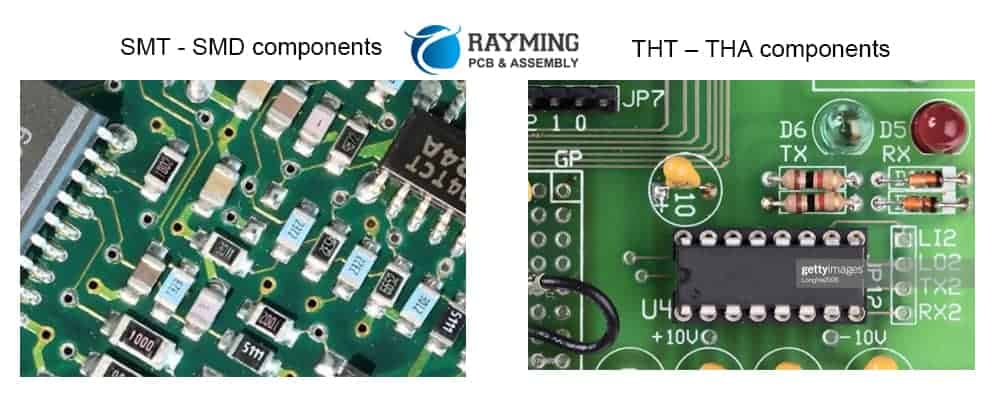
Surface Mount Technology (SMT): Components are placed onto pad surfaces on the outer layers of the PCB and soldered in place. Highly automated pick-and-place machines enable extremely rapid assembly.
Through Hole Technology: Component leads are inserted through holes in the PCB and soldered to pads on the opposite side. More manual assembly, but provides strong mechanical connections.
A combination of SMT and through-hole assembly is common.
What are some key tests conducted during PCB prototyping?
Typical tests conducted on PCB prototypes include:
- Visual inspection – Confirm proper assembly, identify defects
- Flying probe test – Verify electrical connectivity layer-to-layer
- Functional test – Validate circuit behavior/performance
- Environmental stress – Temperature cycling, vibration, etc.
- X-ray inspection – Examine internal layer alignment, voids
- ICT test – Test for short circuits and opens
Thorough prototyping testing helps de-risk moving into production.
How can I avoid common PCB design mistakes?
Some common PCB design mistakes to avoid:
- Violating design rules – Follow fab guidelines to avoid manufacturing issues
- Poor component placement – Optimize placement for routing, heating, etc
- Insufficient board rigidity – Add stiffeners/mounting holes to support components
- Trace antenna effects – Use stitching vias to control unwanted radiation
- Unprotected circuits – Use proper ground planes, spacing, coating, etc.
- Insufficient testpoints – Make boards easy to validate with testpoints
Doing thorough design reviews and prototype testing helps catch many issues.
What file formats are used in PCB manufacturing?
Key file formats include:
- Gerber (.gbr) – Standard for PCB fabrication layer data
- Drill (.drl) – Specifies hole locations and sizes for drilling
- BOM (.csv) – The bill of materials listing components, values, etc.
- Pick-and-place (.csv) – SMT assembly instructions for automated assembly
- IPC-2581 (.pad) – Next-gen intelligent manufacturing data format
Following accepted file standards ensures a smooth manufacturing hand-off.