Introduction
Printed circuit boards (PCBs) are essential components of most modern electronic devices. A PCB mechanically supports and electrically connects electronic components through conductive copper tracks, pads and other features etched from copper sheets laminated onto a non-conductive substrate. PCBs can be single sided, double sided or consist of multiple layers.
The PCB design and assembly process is crucial to creating a functioning electronic device. An overview of the key stages in PCB fabrication is:
- PCB design
- Prototyping
- Fabrication
- Assembly
- Testing
Proper PCB design principles and fabrication techniques are critical for manufacturing a quality PCB ready for component assembly. This article provides a comprehensive guide on PCB design and assembly including the layout, materials, processes, assembly methods and quality standards.
PCB Design
The PCB design stage involves creating schematics and layouts that route connections between components. Effective PCB design requires expertise in electronic engineering and PCB design software.
Schematic Design
A schematic diagram visually represents the components and connections on a circuit using symbols and lines. Schematics should be logical, clear and easy to understand. Common electronic design automation (EDA) software used to create schematics includes:
- Altium
- Eagle
- KiCad
- OrCAD
Schematics should include the target PCB layer structure and stackup, component footprints and logical grouping of circuits by function. Component symbols and reference designators should follow industry standards. Schematics facilitate PCB layout by providing the connectivity map.
PCB Layout
PCB layout involves taking the schematic and translating component positions and connections into a physical board design. Layouts can be completed manually or with EDA software such as Altium and KiCad. Factors considered in PCB layout include:
- Component placement – Laying out parts logically for routing and efficiency
- Routing – Completing copper connections between pads
- Trace width – Widening traces that carry more current based on calculations
- Multi-layer stackup – Organizing signal and plane layers
- Design for manufacturing (DFM) – Following fabrication and assembly rules
Good layout practices include neat right angle traces, 25 mil clearance between conductors, adequate trace widths and spacing electronic components a minimum distance apart.
PCB Materials
PCBs consist of a substrate laminated with a copper layer that is etched into traces and features. The base materials determine the mechanical, electrical and thermal characteristics. The most common are:
Substrates
- FR-4 Glass Epoxy – Most common, cost effective. Glass fabric base with a flame resistant epoxy resin.
- CEM-1 Cotton Epoxy – Low cost, exhibits low moisture absorption. Woven cotton paper base material.
- FR-2 Phenolic – Good electrical properties under high temperatures but brittle. Paper base with phenolic resin.
Copper Types
- Rolled Copper – Formed by rolling copper through successively smaller openings providing good ductility. 1 oz (35 μm) and 2 oz (70 μm) are standard thicknesses.
- Electrodeposited Copper – Plated copper layer with smaller grains, more uniform thickness and better purity. Lower cost.
- Laser-etched Copper – Microline traces etched by laser for widths down to 0.002 inches, high precision.
PCB Prototyping
Prototyping produces initial boards for functionality testing before final fabrication in production volumes. Prototypes verify the PCB layout, components, solder connections and assembly. Common prototyping approaches include:
Breadboarding
A breadboard allows creating rough circuits by plugging components and jumper wires into a plastic board. Quick and inexpensive for initial functional verification.
Wire Wrap
Point-to-point solderless connections using wire ends wrapped around square pins embedded in a substrate. Allows reworking connections and reusing components.
Manhattan Style
A production fabrication method using bare copper boards and hand soldering components like an island arrangement. Fast and simple for small quantities.
PCB Mill/CNC
Using a desktop CNC to mill trace patterns from copper clad laminate boards. Allows fast and inexpensive in-house prototyping.
PCB Fabrication
PCB fabrication transforms the layout into a physical board using processes such as imaging, etching, drilling and plating to form the traces, holes, pads and layers.
Imaging
A photosensitive dry film is laminated onto copper surfaces and patterned using ultraviolet light through a mask printed with the layout. Unexposed areas are later removed during etching.
Etching
Exposes conductive copper from unwanted areas by chemically dissolving using etchants such as ferric chloride or ammonium persulfate.
Drilling
Mechanically drills holes for through-hole component leads using tiny drill bits. Done with CNC drill machines. High density boards may use laser drilling.
Plating
Electrolytic copper plating builds up conductive copper surface to desired thickness. Common for multilayer boards and plated through hole connections.
Soldermask
A protective epoxy based layer with openings for soldering applied over the PCB surface, excluding exposed solder pads. Prevents oxidation and short circuits.
Silkscreen
Prints reference designators, logos and identifying text using an epoxy ink onto the soldermask layer. Improves aesthetics and identifies components.
Electrical Test
Checks for short circuits, opens, and proper functioning of plated through holes via in-circuit or flying probe testing. Ensures quality before component assembly.
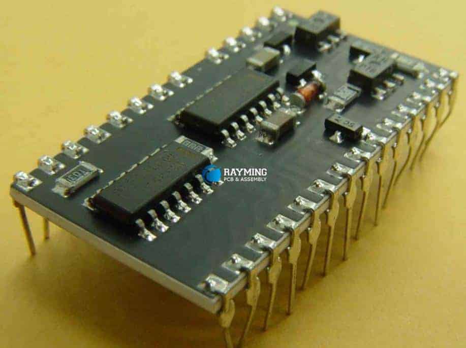
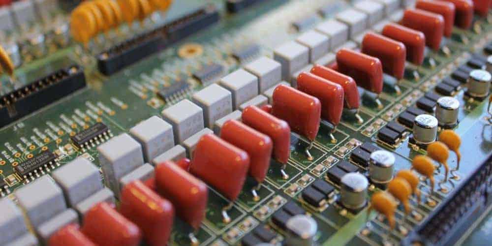
PCB Assembly
Populating PCBs involves mounting and soldering electronic components onto the fabricated bare boards using either manual assembly or automated SMT (surface mount technology) processes.
Manual Assembly
Small quantities use manual PCB assembly with through-hole components, push in wire terminals and connectors. Involves steps like:
- Inspecting boards
- Inserting and orienting components
- Clinching or taping parts to secure before soldering
- Hand soldering each joint
- Clipping excess leads
- Cleaning flux residues
Efficient workmanship and quality control is critical for manual assembly.
SMT Assembly
SMT components have conductive pads that directly attach to matching surface pads on the PCB without leads. High volume production uses automated SMT assembly lines which increase speed, precision and component densities compared to manual methods. The SMT Process includes:
- Solder Paste Application – Dispenses precise solder paste deposits onto pads
- Pick and Place Machines – Robotic placement of tiny SMT components onto pads at high speeds
- Reflow Soldering Ovens – Melts solder paste to form reliable solder joints attaching components
- Automated Optical Inspection – Checks accuracy of placements and quality of solder joints post reflow
- Routing and Hand Assembly – Installs any connectors, headers and through-hole parts
Proper SMT process controls and machine setup helps achieve reliable assembly with close to 0 defects per million opportunities (DPMO).
PCB Testing and Quality Control
Verifying PCB assembly quality requires testing processes like:
- In-Circuit Tests – Applies power and test signals to circuits to check operation and identify faults
- Flying Probe – Tests connectors, vias and traces for opens, shorts and continuity
- X-Ray Inspection – Images internal features like solder joints and alignments
- Boundary Scan – Tests interconnections between components with embedded test logic
- Automated Optical Inspection – Images boards and compares to golden template for assembly defects
- Functional Testing – Validates complete assembled boards operate per the specifications
Quality standards like IPC-A-610 provide acceptability requirements for electronics assembly visual inspections. Statistical process control monitors vital parameters like solder joint quality and thermal profiles during production.
Frequently Asked Questions
What are some key factors to consider during PCB layout?
Some key layout considerations are component placement for efficient routing, trace widths for power transmission, clearance between traces, optimal layer stackup, manufacturability rules and minimizing EMI through ground planes.
What are the differences between FR-4 and CEM-1 PCB substrate materials?
FR-4 glass epoxy is the most common and cost-effective substrate. It uses woven fiberglass inn a flame resistant epoxy resin. CEM-1 uses cotton paper in epoxy resin and exhibits lower moisture absorption but is less common.
What are the benefits of PCB prototyping?
Prototyping allows testing the design, functionality, manufacturability and assembly before final production. This verification avoids costly mistakes if issues are found after launching production.
How accurate are SMT pick and place machines?
Modern high speed pick and place machines achieve placement accuracies within 0.1mm for micro-SMT components. Vision alignment systems precisely locate PCB fiducials for consistent accuracy.
Why is soldermask used on PCBs?
Soldermask prevents solder bridges between closely spaced pads while leaving solderable areas exposed. It also provides insulation, protects against oxidation and improves PCB aesthetics.


0 Comments