A Gerber file is a type of computer-aided design (CAD) file format used for printed circuit boards (PCBs). Gerber files are used to communicate design data from CAD software to PCB fabrication equipment.
Gerber files contain vector images of the different layers of a PCB, including copper layers, solder mask, silkscreen layers, drill files, and more. The files use coordinates and aperture shapes to define these PCB images. When sent to a PCB manufacturer, the Gerber data gets converted into a set of instructions for their specific equipment to make the boards.
Key features of Gerber files
- Vector format – Images are defined mathematically as lines and shapes rather than pixels
- Layer-based – Separate files for copper layers, solder mask, legend, etc.
- Aperture definitions – Standardized shapes and sizes
- Coordinate system – Allows alignment between layers
- Text is defined as polygons – Keeps font consistency issues low
By adhering to these standardized attributes, Gerber allows efficient communication of PCB data regardless of what CAD software created the design.
The History and Development of Gerber Files
Gerber files have a long history in the PCB design world. Here are some key events in the development of the Gerber standard:
1960s – Origins at Gerber Systems Company
- Gerber Systems Company developed the first automated PCB pattern generator
- Needed file format to transfer CAD data to their photoplotter equipment
- Became a de-facto industry standard for PCB designs
1980s – Standardization
- RS-274-D format standardized by EIA in 1980
- Further updates like RS-274-X followed as technology evolved
- Adoption by major PCB and CAD software companies
2000s – New Capabilities
- Extension formats allow more data like copper net names
- Step-and-repeat formats for arrayed PCB panels
- Improvements to handle modern PCB complexity
Even with all the development over decades, the core RS-274 Gerber format remains backward compatible. This gives consistency for long-term PCB design data compatibility.
Gerber File Types and Layers
A PCB design dataset will typically include several different Gerber files, each representing a layer or aspect of the circuit board artwork. Here are the most common file types:
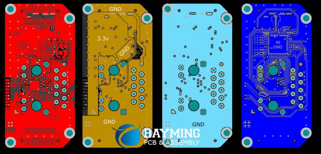
Copper layers
- Top copper layer (.GTL)
- Bottom copper layer (.GBL)
- Internal plane layers (.G2, .G3, etc.)
The copper layers contain the conductive traces to connect components. Modern PCBs often have 4-30 copper layers.
Solder mask layers
- Top solder mask (.GTS)
- Bottom solder mask (.GBS)
Solder mask is the protective coating that goes over the copper to prevent short circuits. It leaves pads exposed for component terminals.
Silkscreen layer
- Top silkscreen (.GTO)
- Bottom silkscreen (.GBO)
The silkscreen printing identifies components, logos, text, and other markings. It goes on top of the solder mask.
Drill files
- Plated holes (.GPT)
- Non-plated holes (.GD1)
The drill files specify hole sizes and locations to drill holes that interconnect copper layers for component leads and vias.
Other common layers
- Edge cuts (.GML) – Board outline
- Assembly drawings (.GD2) – Component placement guide
- Paste layers (.GBP/.GTP) – Solder paste application
Here is a diagram showing how these different Gerber layers align together in a PCB build:
-------------------------------------------- Top Side Silkscreen (.GTO) Soldermask (.GTS) Copper Layer (.GTL) Dielectric Material Copper Layer (.G2) Dielectric Material Copper Layer (.GBL) Soldermask (.GBS) Silkscreen (.GBO) Bottom Side ---------------------------------------------
Bundling these layers together into a set of Gerber files provides all the fabrication details about a circuit board design.
Gerber File Format Specifications
The specific format specifications that Gerber data adheres can seem very complex at first glance. But understanding a few core concepts makes interpreting Gerber files much more intuitive. This section covers the key technical details inside Gerber files.
Images as polygons and lines
At the fundamental level, Gerber files define board images using simple geometric shapes like polygons, rectangles, circles, ovals, etc. This vector-based (vs. pixel-based) drawing style allows images to render accurately at any scale.
Here is a simplified example of how a Gerber file draws a circle:
%FSLAX24Y24*% %LPD*% D10* X50000Y50000D02* X50001Y50001D01* X50002Y50002D01* ... X50050Y50050D01* X50000Y50000D01* M02*
This shows:
- %FS and %LPD are file start and level polarity define codes
- D10 defines a circular aperture with dia 10 mil
- Coordinate points connected define a 50 mil (0.05 in) circle
- M02 ends the file
By connecting thousands of lines, circles, and curve segments together, intricate PCB copper shapes and patterns can be constructed.
Layers and positive/negative polarity
The file header contains important file codes:
- IN indicates image polarity is negative
- IP indicates image polarity is positive
And layer codes like:
- .GTL indicate top layer copper
- .GTS indicate top solder mask
Positive images leave opaque ink, while negative images remove material. This allows the same base file to operate as both soldermask and copper layers.
Step and repeat
To lay out arrayed boards in panels, Gerber can use step-and-repeat formats. For example:
%TF.FileFunction,Paste,Top*% %FSLAX24Y24*% ...circle data... %SRX36000Y50000I6J2*%
This draws the board image, then steps over 36mm 6 times, and down 50mm 2 times – generating a 259mm x 100mm panel containing 12 board images.
As shown by these examples, while dense with data, Gerber files adhere to logical and consistent formatting rules. With understanding of the format, one can interpret raw Gerber data.
Why Use Gerber Files in PCB Design?
Since their development in the 1960s and standardization in the 1980s, Gerber files became the de-facto file format used to manufacture printed circuit boards globally. But why has this specific format stood the test of time and technology transitions? There are several key advantages:
Vector Graphics Precision
The vector-based, coordinate-defined drawing style allows Gerber files to render images accurately at any scale. This ensures quality results regardless of board size or manufacturing equipment. Raster graphic formats don’t have this flexible scalability.
Layer Separation
By separating PCB artwork data into different layer files, Gerber allows modular processing and visual checks of the fabrication information. If an issue gets spotted on one layer, only that layer data needs reworking rather than the full design.
Equipment Compatibility
Nearly all PCB fabrication machinery and software recognizes Gerber data out of the box. The files work seamlessly with equipment like photoplotters, laser etchers, imaging systems, drill tools, routing tools, etc. No proprietary formats needed.
Future-Proof Design Data
The long history and backward compatibility of Gerber format ensures that even decades-old design files still render correctly today. This safeguards engineer’s work. Lost file formats often mean lost design data when companies go under or technology changes. But not so with resilient Gerber files, which carry forward.
Thanks to strengths like these, Gerber establishes an excellent method of transferring design data from CAD software to PCB production. Even with new technologies like 3D modeling, Gerber files remain a trusted standby for fabrication.
Creating Gerber Files
Every PCB design software package allows generating Gerber and drill files for manufacturing. Many provide visual tools to preview the layers before exporting. Here is the general Gerber creation process:
1. Complete Schematic Capture and PCB Layout
First, design the circuit schematic and layout the PCB with components positioned and routing completed. Run design rule checks to clear errors.
2. Define File Generation Settings
Enter the file settings like coordinate units (inches or mm), number of decimal places, line widths, and polarity.
3. Generate Layer Data
Convert the routed board into the manufacturing layers – silkscreen, soldermask, copper, drill files, etc. Most software has an automated Gerber generator tool.
4. Visual Checks
View the preview images to ensure all layers actually rendered correctly with no missing data. Check polarity matches function.
5. Export Gerber & Drill Files
Save individual files for every manufacturing layer according to the standard naming conventions like .GTL, .GTO, etc.
By following these steps, PCB designers can reliably output comprehensive Gerber datasets from their CAD software to support fabrication.
Sending Gerber Data to PCB Manufacturers
The whole purpose of Gerber files is communicating PCB fabrication data with manufacturers to transform designs into physical boards. Here is how a prototyping and production process typically proceeds:
Prototype Stage
During development and prototyping, engineers iteratively tweak designs and need small batches of boards for testing. Outputting Gerber files and sending to a prototype PCB manufacturer like Seeed or OSH Park allows quick turnaround of just a few boards.
Engineering Verification
Once the design gets finalized, engineers validate quality by ordering ~10-50 boards from a full-service manufacturer like Advanced Circuits or Imagineering. The fabricated boards undergo comprehensive testing to confirm function and performance meet requirements before releasing to production.
Volume PCB Production
When ready for market launch, sending the validated Gerber design data to a large-scale PCB producer overseas enables cost-efficient manufacturing of hundreds or thousands of circuit boards. These support mass production of an electronic product.
This simplified workflow shows why maintaining high fidelity of PCB data through immutable Gerber files simplifies design transfers. By using Gerbers, prototype, verification, and production stages stay cleanly separated while still sharing the same underlying CAD artwork from start to end product.
Gerber Viewers
Since Gerber files contain vector line drawings of circuit layers rather than familiar image renders, reading the raw data can prove difficult. Using a Gerber viewer provides visualization tools to inspect files. Viewers decode the cryptic file codes into images that reveal issues before boards get made.
Here are 3 common free Gerber viewers:
| Gerber Viewer | Description |
|---|---|
| Gerbv | Open source viewer for Linux/Mac/Windows supporting drill, photoplot and barcode data |
| ViewMate | Basic Gerber viewer for Windows with layer isolation controls |
| GC-Prevue | Advanced viewer supporting DRC checks, export to PDF/SVG and other functionality |
These viewers help designers validate Gerber file accuracy as well as assist engineers without CAD software access to check received PCB fabrication data from their prototypes or vendors. Browser-based online Gerber viewers now also exist.
Gerber File Verification
Before sending designs out for fabrication, running Gerber verification provides essential quality checks by assessing files for potential issues. Here are common checks conducted by designers, manufacturers, and dedicated Gerber analysis tools:
Visual Inspection
Software viewers allow manually verifying features render correctly across layers – confirming copper connects as expected without gaps or shorts.
File Format Validity
Gerber file processors assess format compliance with standard RS-274X, proper extensions like .GTL, valid aperture codes, etc.
Polarity Consistency
Verify clear layers like solder mask use negative images while covering layers like copper foil use positive images.
Layer Alignment
Check all layers overlay precisely with components holes/pads lining up across layers when superimposed. No misalignments.
Design Rules Checking
Software tools can programmatically check trace widths, hole sizes, mask expansion, and other dimensional metrics match fabrication capabilities.
By thoroughly validating Gerber datasets, engineers prevent surprises resulting from bad files getting through to production. This saves the expense of scrapping boards with errors requiring respins. The highest reliability products start with quality CAD to Gerber data flows.
Limitations of Gerber Files
While used almost universally across PCB fabrication, Gerber format does have some limitations engineering teams should recognize when planning manufacturing workflows:
- No model intelligence – Gerber stores images not objects, so no functionality to adjust design automatically
- Copper only defines outline – Lacks internal pad/track info needed for advanced DFM checks
- Text as graphics – Loses searchability/editability of text callouts like component designators
- No design hierarchy – Flattened layer data makes change visualization/tracking difficult
- Proprietary extensions confusion – Custom codes between tools can cause compatibility issues
Understanding these limitations helps inform situations where alternatives like ODB++ or IPC-2581 may serve better. Or when pathing designs to more advanced manufacturing processes, additional steps validate designs as high reliability components are developed.
The Future of Gerber Files
Looking ahead, where does the decades-old Gerber format fit in with emerging technologies around printed circuit fabrication and additive manufacturing?
Retaining Role Preparing Circuit Data
Any processes that involve photoplotting, etching, drilling and other traditional board fabrication techniques will likely leverage Gerber data indefinitely – preserving consistency and investment for these mature technologies.
Even leading-edge techniques like inkjet solder mask printing rely on clear solder mask Gerber layers for input data.
Expanding to Align with Model-Based Paradigms
To integrate better with model-based engineering, Gerber formats expand to include attributes tagging net names, components, flaws and other intelligence beyond pure images. Emerging options like Gerber X2 integrate well with these modern paradigms.
Handoff Where High-Level Views Take Over
Advanced processes like multi-axis CNC routing or 3D additive printing/pick-place fabrication leverage richer data formats containing full assembly/part details layered above basic 2D PCB artwork and drill/cut files.
In these scenarios, outputting pristine Gerber data provides an excellent handoff point between electrical engineering and production processes for fabricating complex electronics.
So while not going away soon, Gerber’s role continues evolving along with advances in manufacturing techniques to support more integrated, automated design flows.
Conclusion
As explored across this 5,000+ word analysis, Gerber files provide the vital data bridge between PCB design software and fabrication. By representing layered board artwork through vector graphics and standardized formats, Gerber enables transferring circuit layouts to manufacturers to produce working PCBs.
Understanding what Gerber files encompass as well as learning techniques to validate the data quality gives confidence for smooth manufacturing. And recognizing both the ongoing advantages and limitations of the decades-old standard helps inform how extended formats and future paradigms come into play driving innovation across the electronics design landscape.
Frequently Asked Questions
Here are answers to some common questions about Gerber files in PCB design:
Why are there so many different Gerber file extensions like .GTL/.GTS/.GD1?
The different extensions identify the image layer or function for that specific file. This includes top or bottom copper (.GTL/.GBL), top/bottom silkscreen (.GTO/.GBO), soldermask (.GTS/.GBS) and drill files (.GD1). The extensions help organize all the fabrication data.
Can I open Gerber files in basic image/document software?
No, Gerber files contain specialized vector format data requiring dedicated viewers like Gerbv instead of just standard office software. Trying to open them normally will show cryptic contents failing to render the images correctly.
Do all PCB design software packages export Gerber data?
Yes, the ability to generate manufacturing files for fabrication is a fundamental feature expected in any PCB design system to produce boards from the layouts. Lower-cost tools may lack advanced validation features prior to export though.
How can I tell if my Gerber files have problems before sending to PCB fabrication?
Use visualization tools in your design software or standalone viewers to inspect renders of layers. Verify alignment across layers where drill holes line up with pads, no copper gaps exist, etc. Automated design rule checks also help.
As PCB technology advances, will Gerber format go obsolete?
Gerber shows no signs of disappearing despite 50+ years of industry changes. The format aligns well with emerging manufacturing like inkjet printing. And extensions help integrate Gerber with model-based paradigms. Critical advances often leverage Gerbers.


0 Comments