Electronic PCB Assembly: A Complete Guide
Introduction
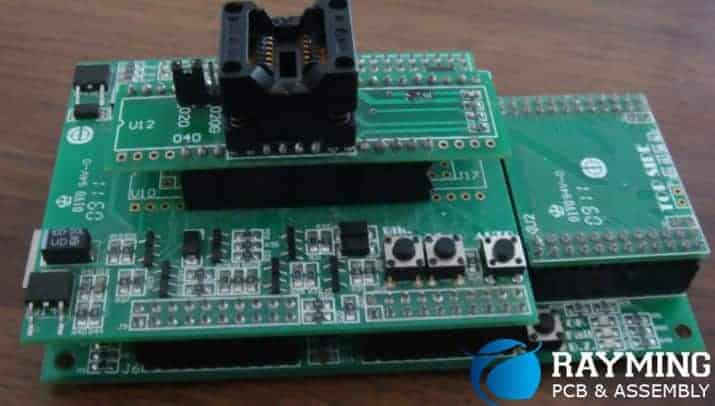
Printed circuit boards (PCBs) are essential components of most modern electronic devices. They provide the physical platform to mount and interconnect electronic components using conductive tracks, pads and other features. The process of assembling the components on the PCB is known as electronic PCB assembly.
Proper assembly is crucial for building functioning electronic devices. This article provides a comprehensive guide on electronic PCB assembly, covering key topics such as:
Overview of PCB Assembly Process
- Steps involved in assembling components on PCBs
- Soldering types and methods
- Cleaning and inspection
- Testing and troubleshooting
Assembly Methods
- Through-hole assembly
- Surface-mount assembly
- Combination method
Facilities and Equipment
- Soldering stations
- Ovens
- Inspection tools
- Testing jigs and fixtures
Quality Control
- Process controls
- Standards and certifications
- Defect detection and correction
Outsourcing Considerations
- In-house vs outsourcing
- Supplier selection criteria
- Managing outsourced projects
By the end of this article, you should have a solid understanding of the PCB assembly process and best practices. Let’s get started.
Overview of the PCB Assembly Process
The assembly process involves mounting electronic components onto the printed circuit board. The main steps include:
1. PCB Fabrication
- The bare PCB is fabricated first. The board has copper tracks to interconnect components.
2. Component Placement
- Components are precisely positioned on the PCB. Often automated pick-and-place machines are used.
3. Soldering
- Components are soldered to the PCB to form electrical connections. Various soldering methods are used.
4. Cleaning
- Flux residues are cleaned off the board after soldering.
5. Inspection
- Assembled boards are visually inspected for defects and quality checks.
6. Testing
- Electrical tests validate proper functioning post assembly.
7. Rework and Repair
- Any defective boards or components are reworked or replaced.
The assembly line is optimized for mass production efficiency, depending on volume and complexity. Let’s look at some key aspects in more detail.
Soldering Types and Methods
Soldering is the main interconnect technology used in PCB assembly. It creates low resistance electrical joints between component leads and copper pads on the PCB. Some key soldering methods include:
Wave Soldering
- Used for through-hole components.
- The assembled PCB passes over a wave of molten solder.
- Solder is applied to all joints simultaneously.
Reflow Soldering
- Used for surface-mount components.
- Solder paste is first applied to pads on the PCB.
- The board passes through a reflow oven.
- The heat melts the solder paste, forming joints.
Manual Soldering
- Used for rework, repairs and low volume.
- Hand soldering iron to target specific joints.
- Requires skilled operators.
Selective Soldering
- Automated soldering of selected points on a PCB.
- Useful for mixed through-hole and SMT boards.
- Achieves flexibility of manual soldering.
| Soldering Method | Description | Advantages | Disadvantages |
|---|---|---|---|
| Wave Soldering | PCB passes over wave of molten solder | Fast process for high volume <br> Low cost | Only for through-hole components <br> Not suitable for fine pitch components |
| Reflow Soldering | Solder paste reflowed by heat | Ideal for surface-mount components <br> High quality joints | Slower process <br> Expensive equipment |
| Manual Soldering | Hand soldering iron used | Flexible <br> Rework and repair | Slow <br> High labor cost <br> Skill dependent |
| Selective Soldering | Automated soldering of selected points | Flexible <br> Combines benefits of wave and manual soldering | Limited to selected joints |
The soldering process must be carefully controlled to achieve reliable joints. Parameters like temperature profiles, conveyor speed, flux chemistry and others are optimized.
Cleaning and Inspection
Cleaning
Post soldering, fluxes and other residues need to be cleaned off the PCBs. Typical cleaning methods include:
- Solvent cleaning with chemical solutions
- Aqueous cleaning using water-based detergents
- Mechanical brushing
- Thermal processes like vapor phase cleaning
Cleaning is critical for removing ionic contaminants and ensuring long term reliability of assemblies.
Inspection
Inspection verifies the quality and correctness of component placement and soldering. It spots defects like:
- Missing or misaligned components
- Poor solder joints
- Physical damage
- Contamination
Inspection techniques include:
- Visual inspection using microscopes
- Automatic optical inspection (AOI)
- X-ray inspection
- Bond pull tests
- In-circuit testing
Testing and Troubleshooting
Testing validates the functionality and performance of the assembled board. It’s done after inspection, and mainly includes:
In-Circuit Testing
- Tests continuity of connections between components.
- Confirms all devices are loaded correctly.
Functional Testing
- Validates overall functionality of the assembled board.
- Uses suitable test signals and loads to check operation.
Burn-In Testing
- Units stressed for prolonged time periods at elevated conditions.
- Used to detect early failures (“infant mortality”).
If testing reveals defects, troubleshooting is done to isolate the fault. Common problems include:
- Cold solder joints
- Dry joints
- Solder bridges
- Wrong components
- Damaged PCB or components
Identifying and rectifying issues is crucial before shipping products to customers.
Facilities and Equipment
Specialized facilities and tools are required for efficient PCB assembly and production. Key equipment includes:
Soldering Stations
- Reflow ovens for SMT assembly. Convection, vapor phase or infrared heating are used.
- Wave soldering machines for through-hole assembly.
- Rework stations for manual soldering.
Board Handling
- Conveyors for moving PCBs through the line.
- Board loaders/unloaders.
- Component storage and feeding mechanisms.
Inspection and Testing
- Microscopes for visual inspection.
- AOI machines for automated optical inspection.
- Flying probe testers for electrical testing.
- Fixtures for burn-in testing.
The assembly line and tools must be selected based on the required production volumes, complexity and quality levels. Automation provides high accuracy at fast speeds.
Quality Control and Standards
Stringent quality control ensures consistent and reliable PCB assembly. Key measures include:
Process Control
- Statistical process control monitors critical parameters.
- Control charts track metrics like defects per board, yield and test pass rate.
- Out-of-control conditions are fixed.
IPC Standards
- IPC standards like IPC-A-610 set quality requirements for electronics assembly.
- Criteria define acceptable and defective conditions for parameters like solder joint quality, cleanliness, component damage etc.
ISO Certification
- Many PCB assembly facilities get ISO 9001 certified.
- This validates quality systems and process capability.
Defect Reduction
- Continuous improvement programs focus on reducing defects.
- Analysis tools like pareto charts identify vital few causes to control.
- DFM reviews help optimize board design for manufacturability.
Following best practices for quality PCB assembly reduces field failures and warranty costs.
In-House Assembly vs Outsourcing
For most companies, outsourcing PCB assembly to specialized providers is the preferred model. Key factors when deciding between in-house vs outsourcing include:
In-House
- Better control over quality and IP protection
- Faster turnaround on new product intros & changes
- Lower unit costs at high volumes
In-house only makes sense for very high volumes, proprietary products, or mission-critical applications where quality control is paramount.
Outsourcing
- Access to advanced assembly technologies
- Leverage assembly expertise and best practices
- Faster time-to-market
- Lower costs for medium volumes
- Focus on core competencies rather than assembly processes
Outsourcing is suitable for most applications. However, the contract manufacturer (CM) must be selected carefully based on capabilities, quality, costs and other factors.
Selecting and Managing Outsourced Assembly
When outsourcing PCB assembly, follow these steps for best results:
Set Clear Requirements
- Define product specs, quality standards, acceptance criteria, test procedures etc.
- Get thorough technical quotations from CMs based on requirements.
Evaluate Supplier Capabilities
- Audit CM’s facilities, processes, staff and certifications.
- Review their experience on similar projects.
- Validate sample builds.
Design for Manufacturability
- Work with CM engineers on DFM analysis.
- Optimize board design to avoid assembly issues.
Manage the Project Actively
- Have regular checks to ensure progress as per schedule.
- Get updates on technical issues during builds.
- Review process quality data.
- Validate deliverables at each stage.
Build Long Term Partnerships
- Don’t frequently switch suppliers.
- Work together to improve processes.
- Share technical knowledge and staff skills.
This enhances quality, reduces costs and establishes productive long-term partnerships with suppliers.
Frequently Asked Questions
Here are some common FAQs about electronic PCB assembly:
Q1. What are the most common PCB assembly defects?
Some typical assembly defects are:
- Missing, wrong or damaged components
- Poor solder joints – cracks, insufficient wetting
- Solder bridges
- PCB damage – scratches, nicks, burnt spots
- Contamination from flux or other residues
Q2. How are packaged semiconductors assembled on PCBs?
Packaged ICs and transistors are assembled by:
- Precise component placement using pick-and-place machines
- Reflow soldering to solder package leads to pads on the PCB
- For BGAs, solder balls on the package connect with pads on the PCB
Q3. What is the difference between through-hole and SMT PCB assembly?
Key differences:
- Through-hole – Leaded components, wave soldering
- SMT – Small leadless components, reflow soldering
- SMT needs expensive pick-and-place machines but allows greater miniaturization and higher component density.
Q4. How can defects be minimized during PCB assembly?
Defect reduction strategies include:
- Statistical process control
- Improved process capabilities
- Operator training
- Inspection at multiple stages
- Testing of assemblies
- DFM reviews to optimize design
Q5. What are some best practices to manage outsourced PCB assembly projects?
Recommended best practices include:
- Clearly defining technical requirements and acceptance criteria
- Thorough supplier evaluation and sampling
- Regular progress monitoring and technical reviews
- Optimizing design for manufacturing
- Building long-term strategic partnerships
- Knowledge sharing between supplier and buyer teams
Following these practices improves quality and collaboration in outsourced PCB assembly projects.
Conclusion
PCB assembly transforms a bare printed circuit board into a functional electronic device. The process demands expertise in specialized technologies like soldering, cleaning, inspection and testing. Outsourcing assembly to contract manufacturers enables access to advanced capabilities and focuses internal resources on product design and core competencies. By following the guidelines in this article for process control, quality management and supplier selection, companies can build high-quality and reliable electronic products cost-effectively.


0 Comments