Introduction
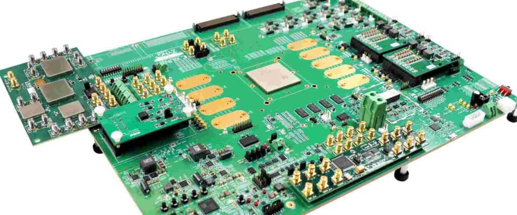
Printed circuit boards (PCBs) form the backbone of most modern electronic devices. From smartphones to appliances, PCBs provide the interconnects between components that allow devices to function. Over the past few decades, surface mount technology (SMT) has become the predominant method of assembling PCBs. In SMT, components are mounted directly onto the surface of the PCB rather than through holes. This article provides a comprehensive overview of SMD (surface mount device) PCB assembly for electronics manufacturing.
Overview of SMT and SMD Technology
SMT emerged in the 1980s as an alternative to through-hole technology, where component leads are inserted into holes drilled in the PCB. SMT provides several advantages:
- Higher component density – Components take up less space on the board surface than through-hole parts
- Smaller components – Chip resistors, capacitors, and ICs can be made much smaller
- Automated assembly – Pick-and-place machines enable fast, automated SMD population
- Double-sided mounting – SMDs can be placed on both sides of a PCB
- Improved reliability – No inserted leads means less potential for failure
- Faster production – SMT streamlines manufacturing, increasing throughput
SMD (surface mount device) refers to the components designed for SMT. Common SMD component types include:
- Chip components – Resistors, capacitors, transistors
- SOICs – Small-outline integrated circuits
- SOTs – Small-outline transistors
- QFNs – Quad flat no-lead packages
- BGAs – Ball grid arrays
- CSPs – Chip-scale packages
SMDs feature conductive terminals designed for surface mounting, like pads, balls, or leads on the underside. Their small size and standardized packaging make SMDs ideal for automated assembly.
SMD PCB Assembly Process Overview
SMD PCB assembly involves mounting and soldering SMDs onto printed circuit boards using SMT equipment. The main steps are:
- SMD placement – SMDs are picked from feeders and precisely placed onto PCB pads
- Solder paste printing – Solder paste is applied to PCB pads where components will be placed
- SMD attachment – The PCB travels through a reflow oven, melting the paste to attach components
- Inspection – Automated optical inspection (AOI) checks for defects
- Testing – Testing validates proper function after assembly
- Conformal coating (optional) – A protective coating can be applied
This sequence of steps is illustrated below:
Key Steps in Detail
Let’s explore the most important stages of SMD PCB assembly in greater depth:
SMD Placement
During SMD placement, pick-and-place machines mount components onto PCBs precisely and rapidly. Feeders or tapes supply components to the pick-and-place head, which uses vacuum nozzles to pick parts before placing them in their designated locations on the board.
High-speed pick-and-place systems can mount tens of thousands of components per hour. Accuracy down to 0.025mm or lower ensures components are optimally positioned. Vision systems align parts and circuit boards using fiducials and other features.
Solder Paste Printing
Solder paste is a mixture of solder powder, flux, and a binding agent that enables SMD attachment. Prior to SMD placement, solder paste is printed in a pattern that matches the component pads on the PCB. Stencils or screens precisely transfer the paste to the required locations.
Printing solder paste facilitates mounting of micro-scale components and ensures reliable electrical connections. Modern solder paste printers deliver high accuracy and repeatability at high speeds.
SMD Reflow Soldering
After paste printing and component placement, solder paste is melted to create permanent solder joints. Reflow soldering uses thermal profiles with different zones to gradually heat SMDs and attach them. Typical SMD reflow involves:
- Preheating – Warms the assembly to reduce thermal shock
- Soaking – Heats assembly to soldering temperature
- Reflow – Peak temperature melts the solder paste, wetting pads and leads
- Cooling – Hardens solder joints, completing electrical connections
The solder paste reflow process is illustrated below:
Most SMD reflow soldering uses convection ovens with forced airflow heating. The PCB moves through different temperature zones on a belt or conveyor. For small volumes, hot plates, infrared heaters, or soldering irons can reflow solder paste.
Post-Solder Cleaning
After soldering, any remaining flux residue is cleaned from the PCB assembly using appropriate cleaning agents. Cleaning removes impurities that could otherwise cause issues like electrical shorts or corrosion. Common SMD cleaning methods include:
- Solvent cleaning – Using detergent solutions or pure solvents
- Aqueous cleaning – Immersion tanks or spray washing with water-based cleaners
- Laser cleaning – Ablating residue with lasers
- Plasma cleaning – Using ionized gas plasma to disintegrate contaminants
- Mechanical cleaning – Brushing or agitating assemblies
Thorough cleaning is essential for reliability, though many low-residue flux pastes require minimal post-solder cleaning.
Automated Optical Inspection
Once soldered, PCB assemblies undergo automated optical inspection (AOI). AOI systems use high-resolution cameras to check assemblies for defects like missing or misaligned components, insufficient solder, and PCB damage.
Some key capabilities of AOI include:
- 3D scanning – Creates height maps identifying soldering defects
- Pattern matching – Compares boards to ideal templates
- Model-based inspection – Checks against 3D computer models
- Statistical process control – Detects process deviations
- Programming flexibility – Supports frequent product changeovers
By rapidly inspecting assemblies, AOI prevents defective products from progressing further. This improves quality control and minimizes costs.
Testing
After assembly, PCBs undergo electrical and/or functional testing relevant to the specific application. Typical tests include:
- In-circuit testing – Validates connections between components
- Flying probe testing – Checks continuity between test points
- Boundary scan testing – Uses on-chip infrastructure to test interconnects
- Functional testing – Confirms operation of the populated board
- Burn-in testing – Stresses components to identify early failures
Rigorous testing provides a final reliability and performance check before shipment. Feedback from testing also helps refine processes.
Conformal Coating
For added protection, a conformal coating can be applied to assembled PCBs. Polymeric coatings like acrylics, urethanes, or silicones deposit a thin protective layer over the entire assembly. Benefits include:
- Insulation – Prevents short circuits
- Moisture resistance – Protects against environmental damage
- Mechanical stability – Improves shock/vibration tolerance
- Chemical resistance – Guards against corrosion
Conformal coatings safeguard assembled PCBs from dust, moisture, and other contaminants during operation. Both selective and full board coating can be performed automatically.
SMD PCB Assembly Equipment
Specialized equipment is essential for high-volume SMD PCB production. Here are some of the key tools for SMT assembly:
SMD Pick-and-Place
As described earlier, pick-and-place systems rapidly and accurately populate PCBs with components. Top pick-and-place machines offer:
- High speed – 100,000+ SMD placements per hour
- Excellent accuracy – +/- 0.025 mm precision or better
- On-the-fly nozzle changing
- Broad component range – 01005 chips to large connectors/BGA packages
- Advanced vision alignment – fiducial recognition, pattern matching, etc.
Leading manufacturers include Fuji, Panasonic, Assembleon, Juki, and Universal Instruments.
Solder Paste Printer
Solder paste printers deposit paste in complex patterns through stencils or screens. Precision printers offer:
- Fine pitch capability – Prints patterns down to 0.1mm pitch
- High accuracy – Alignment +/- 50 microns
- Stencil cleaning – Automatic understencil cleaning
- Easy changeovers – For quick stencil/PCB swaps
- Closed-loop adjustment – Automatic print verification and correction
- High speed – Up to 150mm/sec board motion
Prominent solder paste printer vendors are DEK, Speedline, and MPM.
Reflow Oven
As covered earlier, reflow ovens attach SMDs by melting solder paste. Modern ovens provide:
- Multi-zone heating – Separate preheat, soak, reflow, and cool-down zones
- Forced convection – Heat transfer using fans
- Profiling capabilities – Closed-loop thermal process control
- Inline configuration – Continuous processing
- Fast ramp rates – Up to 5??C/second
- Suitable for lead-free soldering profiles – Peak temperatures up to 260??C
Well-known suppliers are Rehm Thermal Systems, Heller, ERSA, and Folungwin.
Inspection Systems
AOI machines quickly identify defects after soldering. Advanced systems feature:
- Dual-lighting – Simultaneous top and bottom illumination
- 3D inspection – Height measurement to detect poor joints, coplanarity, etc.
- false call reduction – Minimizes false rejects
- Easy programming – From CAD data, macros, etc.
- Wide viewing area – Up to 510 x 510mm
- High resolution – Up to 25 microns/pixel
- High throughput – 3000+ cm??/hour inspection rates
Leading AOI companies are Koh Young, Mirtec, ViTrox, and CyberOptics.
Key Factors for Quality Assembly
Achieving consistently high-quality SMD assembly requires attention to many parameters:
- Component packaging – Moisture sensitivity levels, tape-and-reel quality, etc.
- Material selection – PCB laminates, solder paste alloys, coatings, etc.
- PCB design – Land patterns, density, fiducials, etc.
- Stencil design – Aperture size/shape, thickness, layout, etc.
- Solder paste – Alloy, particle size, flux chemistry, etc.
- Assembly process – Adherence to thermal profiles, pressure, times, etc.
- Cleanliness – Preventing contamination during production
- ESD control – Static protection for sensitive components
- Inspection rigor – AOI detection capabilities, operator training, etc.
- Qualified personnel – Skilled machine operators and process engineers
By holistically optimizing all aspects of assembly, manufacturers can achieve high yields with near-zero defects.
Advantages of SMD PCB Assembly
The SMT assembly process provides significant benefits over through-hole PCB manufacturing:
- Miniaturization – Chips and components can be made much smaller
- Higher density – More components packed in less space
- Simplified automation – Pick-and-place lends itself to automation
- Lower labor requirements – Reduced manual intervention
- Faster speeds – Higher production throughput
- Double-side mounting – Components can be placed on both sides
- Improved testability – Smaller components facilitate testing
- Environmental resistance – SMT joints eliminate inserted leads susceptible to vibration/corrosion
These advantages enable smaller, lighter, more capable, and more reliable electronics products. SMT has allowed the commercialization of devices like smartphones that would not be feasible with through-hole assembly.
Summary
- SMD PCB assembly involves mounting and soldering SMDs onto circuit boards using surface mount technology.
- Key steps include SMD placement, solder paste printing, solder reflow, cleaning, AOI, and testing.
- Specialized equipment like pick-and-place systems and reflow ovens is required for high-volume production.
- Attention to many parameters like packaging, materials, stencil design, and process controls ensures assembly quality.
- Compared to through-hole assembly, SMT provides major benefits like miniaturization and simplification of automation.
SMD technology and assembly processes will continue advancing to accommodate needs for denser, faster, and more capable electronics. Robust process knowledge paired with the latest equipment lays the foundation for efficient, high-yield PCB assembly.
Frequently Asked Questions
What are the main advantages of SMD PCB assembly?
The key advantages of SMD assembly include:
- Higher component density – Small SMDs take up less space than through-hole parts
- Miniaturization – Components can be made extremely small
- Simplified automation – Standardized SMDs enable easier pick-and-place
- Faster production – SMT streamlines manufacturing steps
- Double-side mounting – SMDs can be placed on both sides of a PCB
- Improved reliability – No fragile inserted leads prone to failure
What is the role of solder paste in SMD assembly?
Solder paste provides adhesive to hold components in place on the PCB and solder to create electrical connections after reflow. Precise solder paste deposition is critical for successful SMD assembly.
What is the difference between SMT and SMD?
SMT (surface mount technology) refers to the assembly technique of mounting components directly onto the PCB surface. SMD (surface mount device) refers to the type of electronic components designed for SMT assembly.
What inspection methods are used to validate SMD assembly?
Automated optical inspection (AOI) is the primary inspection method. AOI uses cameras to rapidly check assembled PCBs for defects. Other methods like in-circuit testing or x-ray inspection provide supplementary inspection.
How are components supplied for SMD placement?
Components are supplied on tapes or in trays to SMD pick-and-place machines. Tapes allow continuous feeding of small components while trays provide stacks of larger parts


0 Comments