Introduction to SMT Manufacturing
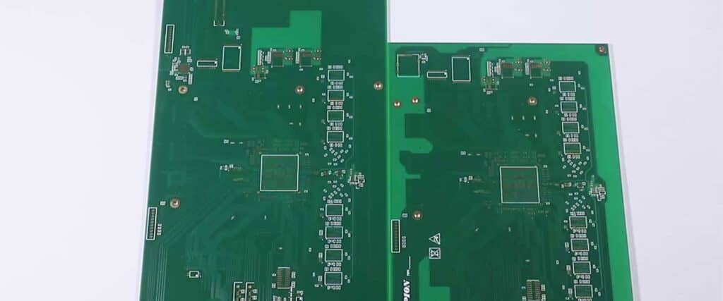
Surface mount technology (SMT) is a method of producing electronic circuits where components are mounted directly onto the surface of printed circuit boards (PCBs). SMT has largely replaced the older through-hole technology, where components were inserted into holes drilled in the PCB. There are several advantages to SMT:
- Smaller components – SMT components can be much smaller than their through-hole counterparts. This allows for greater component density on the PCB.
- Automated assembly – SMT is highly suited to automated assembly, improving production speeds and reducing labor costs.
- Improved performance – Smaller components and higher density result in shorter signal paths, allowing SMT circuits to operate at higher frequencies.
The transition from through-hole to SMT led to a revolution in electronics manufacturing. In this article, we’ll take a detailed look at the SMT manufacturing process and the key steps involved.
SMT Components
SMT components are designed to be soldered directly to the surface of a PCB. Some of the most common SMT component types are:
- Chip resistors and capacitors – Tiny passive components just a few mm in size. Available in standard sizes like 0201, 0402, and 0603.
- SMT resistors and capacitors – Larger passive components, similar in size to through-hole parts. May have leads for added stability.
- Quad flat packages (QFPs) – Integrated circuits with leads extending from the sides. Range from 20 to several hundred leads.
- Ball grid arrays (BGAs) – ICs with leads arranged in a grid on the bottom surface. Soldered via an array of solder balls.
- Chip-scale packages – Extremely compact ICs nearly the same size as the silicon chip inside. Includes flip-chip and wafer-level packaging.
Other SMT component types include transformers, inductors, connectors, LEDs, and various sensors and transducers.
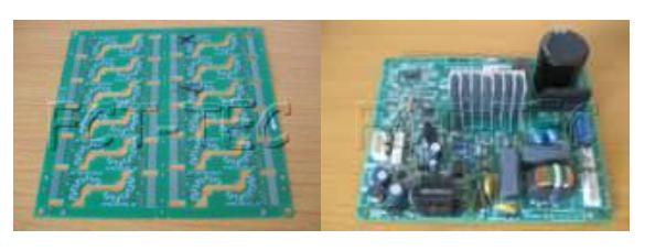
SMT PCB Design
Printed circuit boards designed for SMT differ from traditional PCBs in a number of ways:
- Pads are much smaller to match the leads on SMT components. There are no plated through-holes.
- Pads and traces are spaced very close together to maximize component density.
- Smaller trace/space width and thinner copper layers enable fine features.
- Soldermask openings leave PCB pads exposed for soldering.
- Fiducials provide alignment targets for automated assembly.
- Testing points are interspersed to check for manufacturing defects.
Many of these PCB design factors help facilitate automated assembly and inspection of SMT boards.
Land Patterns
The land patterns – the copper pads that components are soldered to – are designed specifically for each component package type. The size, shape, and spacing of pads matches the leads or balls on the bottom of SMT components. This helps control the final solder joint shape and quality.
Here are some examples of SMT land patterns:
| Component | Land Pattern |
|---|---|
| QFP | Show Image |
| BGA | Show Image |
| 0402 resistor | Show Image |
Soldermask and Pastemask
The soldermask is a key design layer that coats the entire PCB except for areasrequiring solder. Openings in the mask expose the component pads. The pastemaskworks similarly but controls where solder paste is printed during assembly.
Proper soldermask and pastemask design ensures accurate solder deposition and joint formation. The mask openings are typically slightly larger than the pads to account for registration tolerance. This prevents bridging defects.
SMT Stencils
Solder paste is applied to PCBs through metal stencils before component placement. Thestencils are laser cut with apertures matching the solder paste layer from the PCBdesign files.
High precision laser cutting and electroformed nickel/stainless steel construction ensure the stencils mate accurately with PCBs during solder printing. Stencils have a typical thickness around 4-5 mils. Thicker stencils deposit more solder paste.
The interior walls of stencil apertures are also important. A laser cut provides a trapezoidal cross-section which helps release solder paste from the stencil. Electropolishing smoothes surface roughness to prevent paste sticking to the walls.
Solder Paste Printing
Solder paste printing deposits small globs of solder paste on SMT pads through the apertures in the stencil. An accurate print lays down the right amount of solder for each component. There are three main printing methods:
Stencil Printing
This uses a squeegee blade to sweep solder paste across the stencil surface, forcing it into openings. Stencil printers offer high speed and volume production printing.
Dispensing
Precision solder paste dispensers can be used for lower volume jobs. They utilize pressurized systems and valves to deposit controlled dots or lines of solder. Dispensing yields less waste compared to stencil printing.
Jet Printing
In jet printing, solder paste is forced out through narrow nozzles using piezoelectric, thermal, or pneumatic actuation. Nozzles can be arranged in arrays for fast on-the-fly printing. Height sensing maintains constant print height.
SMT Component Placement
SMT components are precisely placed onto solder paste deposits using automated pick and place systems. These machines use vacuum nozzles to pick components from reels, trays, sticks and other sources and position them on PCBs with accuracy up to 0.1mm.
Advanced placement systems offer production rates exceeding 35,000 components per hour. They utilize computer vision alignment and correction to match components to PCB fiducials.
Solder Reflow
After solder paste printing and component placement, PCBs enter the reflow oven to form solder joints. Different heating methods are used:
- Convection ovens – Heated forced air, good for small volumes
- Vapor phase reflow – Condensation and evaporation of an inert liquid
- Infrared reflow – Fast heating with infrared lamps or panels
The reflow profile – the temperature vs. time curve – is carefully set to ensure good wetting and shaping of solder joints without damaging components. The process melts solder paste deposits, allowing surface tension to pull components into alignment.
Inspection and Testing
Automated optical inspection (AOI) systems are used throughout the SMT assembly process to check for defects:
Pre-reflow – inspects paste printing quality and component placement Post-reflow – verifies all solder joints are formed without any bridging between pads
For electrical testing, “bed of nails” test fixtures make contact with test points on assembled PCBs. Testing checks the board for short circuits, open traces, and proper functioning of the circuit.
Rework and Repair
Despite rigorous quality control, some assembled PCBs will inevitably require rework and repair:
- Reflow – Running board through oven again to re-melt faulty solder joints
- Solder wick – Braided copper tool to remove excess solder bridges
- Soldering iron – Hot air station for component removal and replacement
- Automated repair – Machine precision removal and replacement of components
Proper rework improves manufacturing yields and prevents wasting fully-assembled PCBs due to minor defects.
Common SMT Defects
Some of the most frequent defects encountered in SMT production include:
Solder bridging – Solder forms between adjacent pads causing shorts. Can arise from inaccurate paste printing or component tilt.
Solder balls – Small blobs of solder that collect from splashing or residue. Can cause shorts.
Tombstoning – Chips or components that stand up during reflow. Leads to incomplete joints.
Voids – Air gaps within solder joint, reducing strength. Caused by outgassing during reflow.
Solder beading – Excess solder builds up on one side of joint. Can lead to bridges.
Advantages of SMT
Some key advantages of surface mount technology:
- Small component sizes promoting miniaturization of electronics
- Extremely high component density – up to 1000 components per square inch
- Majority of components placed by fast automated processes
- Greatly reduced handling compared to through-hole assembly
- Shorter electrical paths enable high speed circuit operation
- Minimal waste and lead consumption compared to through-hole
SMT enables advanced circuit miniaturization and helps meet demands of modern electronic product design.
Disadvantages and Challenges
SMT does have some disadvantages and production challenges:
- Sensitive to dust, temperature variation, vibration. Tight process control needed.
- Solder joints can crack more easily under thermal cycling loads.
- Replacing faulty components without damage is very difficult.
- Dense PCB layouts complicate trace routing, thermal design, RF performance.
- Expensive equipment cost for high-speed automated assembly.
- Requires technical expertise to troubleshoot assembly defects.
The Future of SMT
While SMT manufacturing has matured considerably, advances continue to be made:
- Even smaller 01005 and 008004 chip components
- MicroLEDs just 10-100 microns in size
- Warpage-resistant PCBs to prevent chip cracking
- Extremely fine pitch components down to 0.3mm spacing
- Inkjet printing of solder paste and adhesives
- More environmentally friendly water-soluble solder pastes
- Automated optical inspection using artificial intelligence
- Major strides toward fully automated “lights out” factories
Continued SMT developments will enable functionality and performance gains in nearly all types of electronic products.
SMT Manufacturing FAQ
Here are some frequently asked questions about surface mount manufacturing:
What are the key differences between through-hole and SMT production?
The main differences are:
- SMT components are much smaller, enabling miniaturization and high density
- SMT Eliminates need to drill holes in PCBs
- SMT is optimized for automated assembly with machines
- SMT typically uses solder paste instead of wave soldering
- Quality control is heavily reliant on automated optical inspection
How are very small chip components handled and picked up by SMT machines?
Specialized feeders supply tiny chip parts like 0201 size resistors. Parts stick to the carrier tape through static electricity rather than mechanical features. The pick and place nozzle uses an optical recognition system to locate and pick parts. A vacuum hole provides suction to lift and place the small component.
Why does tombstoning occur and how can it be prevented?
Tombstoning happens when the surface tension of molten solder pulls a chip upright during reflow. It can be prevented by:
- Using the correct pad size for good wetting of both leads
- Having plated lead-in chamfers to guide solder flow
- Optimizing paste volume and position for symmetric reflow
How are BGA packages soldered, given they have no visible leads?
BGAs are soldered via the array of tiny solder balls on the underside of the package. Solder paste is printed on PCB pads matching the ball positions. During reflow the balls re-flow and create connections to the PCB through surface tension. X-ray inspection verifies ball attachments.
Why is process control so critical in SMT?
With very small components and minimal solder, there are tight tolerances involved in SMT. Variations in stencil/PCB alignment, paste deposition, placement accuracy, and reflow profile can easily cause defects like bridges or poor joints. Tight control over equipment, materials, and environment is needed.
This FAQ covers some key aspects of SMT manufacturing technology. Please let me know if you would like me to expand on any part of the article!


0 Comments