Introduction
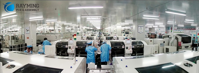
Printed board assembly, also known as PCB assembly, is the process of soldering and assembling electronic components onto a printed circuit board (PCB). PCB assembly is an essential step in manufacturing electronic devices and components. In this comprehensive guide, we will explore what PCB assembly involves, its importance in electronics manufacturing, the assembly process step-by-step, and tips for choosing the right PCB assembly service provider.
What is Printed Board Assembly?
Printed board assembly refers to the process of soldering and connecting electronic components like capacitors, resistors, integrated circuits onto the surface of a PCB using solder. The PCB acts as the foundation on which components are assembled to form a functional electronic circuit.
PCB assembly involves placing components accurately on conductive copper pathways on the board surface called traces. Components are then soldered to these traces to create a complete electronic circuit. This assembled PCB is tested for functionality before being integrated into electronic devices and products.
Why is PCB Assembly Important?
Here are some key reasons why PCB assembly is a crucial process in electronics manufacturing:
- It transforms a bare PCB into a fully functioning electronic circuit board.
- It facilitates installation of components like ICs, transistors, etc. onto the PCB.
- It electrically and mechanically connects components to the conductive pathways on the PCB.
- It ensures reliability of connections between components.
- It is a prerequisite for testing and troubleshooting of the populated PCB.
- It is required to integrate the assembled PCB into electronic products.
In essence, PCB assembly converts raw PCBs into functional electronic assemblies that power various devices and components.
PCB Assembly Process Step-by-Step
The printed circuit board assembly process involves several key stages:
1. PCB Design and Fabrication
The first step is designing the PCB layout and schematics using EDA software like Altium, Eagle, OrCad, etc. Once the design is finalized, the actual PCB fabrication takes place. Bare PCBs are manufactured by PCB vendors based on these designs.
2. Stencil Fabrication
A metal stencil with cutouts of the exact shape and size of component pads/footprints is created. This stencil aids in applying solder paste accurately onto the PCB during assembly.
3. Solder Paste Application
The stencil is aligned over the PCB and solder paste is applied on all points requiring soldering. This pre-deposits the paste which will form solder joints subsequently.
4. Component Placement
Electronic components are accurately placed on their designated pads as per the PCB design using machines or by hand. Care is taken to orient polarized components correctly.
5. Reflow Soldering
The PCB goes through a SMT reflow oven heat cycle causing the solder paste to melt and create electrical joints between components and copper traces.
6. Post-Solder Cleaning
Any solder flux residue is cleaned off the PCB using solutions leaving clean, reliable solder joints.
7. Conformal Coating
A protective insulating acrylic coating may be applied on the assembled board leaving only points that allow external electrical connections.
8. Testing and Inspection
The fully assembled PCBs are tested thoroughly to validate their functionality. Automated optical inspection is done to check for defects.
9. Integration and Use
The assembled PCBs are finally integrated into electronic appliances, devices and products in which they provide the desired functionality.
Types of Electronic Components Used in PCB Assembly
Here are some of the main types of components that are soldered onto PCBs during assembly:
- Passive Components – Resistors, capacitors, inductors, transformers, diodes, crystals, fuses, etc.
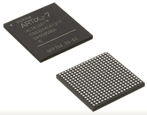
- Active Components – Transistors, integrated circuits (ICs), LEDs, microprocessors, microcontrollers, etc.
- Electromechanical parts – Switches, relays, connectors, sockets, heat sinks, etc.
- Power Supplies – Voltage regulators, power transistors, rectifiers, batteries.
- Wire and Cables – For making off-board electrical connections.
Choosing a PCB Assembly Service Provider
For companies producing electronic products, it is typically more feasible to outsource PCB assembly to a specialized service provider rather than do it in-house. Here are some tips for selecting an EMS company for PCB assembly services:
- Choose an experienced company with good reputation in the industry.
- Ensure they have capabilities for both traditional and SMT assembly.
- Evaluate their production capacity and lead time commitments.
- Look for ISO-certified manufacturers who follow quality protocols.
- Review their component sourcing, procurement and inventory management.
- Assess their testing and post-assembly services like device programming.
- Consider the range of assembly volumes they support – from prototypes to mass production.
- Ensure they have robust security and IP protection measures.
- Understand their pricing and payment terms clearly upfront.
Advantages of Outsourced PCB Assembly
Partnering with a reliable EMS company for PCB assembly offers multiple benefits:
- Cost Savings – Eliminates expenses involved in maintaining in-house SMT assembly lines.
- Focus on Core Competencies – Allows OEMs to focus on design and core product development.
- Fast Time-to-Market – Enables quick prototyping as well as ramping up to mass production.
- Quality – Leverages expertise and quality best practices of specialized assembly firms.
- Reliability – Ensures consistency and repeatability using process-oriented approaches.
- Scalability – Offers flexibility in production volumes to meet changing market demands.
- Latest Technology Access – Utilizes state-of-the-art machines, equipment and processes.
Key Factors Impacting Cost of PCB Assembly
The total cost of getting PCB assembly done depends on various factors:
Component Factors:
- Type of components – SMT vs through-hole
- Size of components
- Number of unique component types
- Standard vs custom/complex components
Design Factors:
- PCB density – More components clustered together increase cost
- PCB size
- Number of PCB layers
- Fine-pitch components requiring advanced assembly
Production Factors:
- Quantity of PCBs being assembled in a batch
- Lead time available for assembly
- Testing and inspection requirements
- Special processing requirements like coating, programming, etc.
Service Provider Factors:
- Their capabilities, capacity and technologies
- Level of automation
- Geographic location
Understanding PCB assembly cost drivers enables creating an optimal assembly strategy.
How Long Does PCB Assembly Take?
A typical assembly time estimate for small to medium volumes of simple PCBs is around 2-3 days with an experienced assembler in Asia.
For complex boards and large scale production runs, procurement of components takes longer driving up overall turnaround time.
Rushed/urgent orders also usually involve higher costs to prioritize them and expedite certain processes.
Here is a quick look at indicative timelines:
| PCB Assembly Stage | Duration |
|---|---|
| Sourcing Components | 2-5 days |
| Solder Paste Stenciling | 1-2 days |
| SMT Pick and Place | 1-2 days |
| Reflow Soldering | Same day |
| Cleaning/Coating | 1 day |
| Testing/QC | 1-2 days |
| Total Time | 2-3 days (typical)<br>Up to 2 weeks (complex PCBs) |
Trends in Electronics Assembly Technology
Some key trends shaping PCB assembly currently are:
- Growth in multi-layer PCBs with 4-6 layers or more necessitating vias-in-pad.
- Miniaturization driving demand for assembling ultra-fine pitch 0201 and 01005 components.
- Higher assembly precision with computer and machine vision guided placement.
- Automating inspection using 3D optical inspection systems.
- Advances in SMT pick-and-place speed, accuracy and flexibility.
- Mainstream adoption of no-clean lead-free soldering.
- Increased use of surface mount over through-hole assembly.
- Environmentally friendly manufacturing processes.
Frequently Asked Questions
Q: What is the difference between PCB fabrication vs PCB assembly?
PCB fabrication refers to making the bare printed circuit board from substrate materials using processes like etching. PCB assembly involves soldering components onto the fabricated PCB. Both steps are crucial in PCB manufacturing.
Q: Can PCB assembly be done by hand?
Yes, PCB assembly can be done manually using soldering irons, magnifying lenses, tweezers, etc. But it is tedious, slow and prone to errors. Automated SMT assembly is preferable as volumes increase.
Q: What is the typical failure rate for assembled PCBs?
With stringent quality control practices, failure rates of 0.1% – 3% are common during PCB assembly. This may vary based on production volumes, complexity, component types used etc.
Q: Should rework/repair be expected during PCB assembly?
Minor rework like touching up solder joints may be needed on some boards after inspection. But well-optimized assembly processes should minimize the overall rework rate typically to 2-5%.
Q: Can assembled PCBs be customized post-production?
Yes, PCBs can customized by cutting access windows, edge-plating, conformal coating select areas, potting, programming firmware, lasering markings etc. based on customer requirements.
Conclusion
PCB assembly is a complex, specialized process that requires expertise and precision in accurately soldering a wide array of components onto PCBs. Partnering with an experienced, high-quality PCB assembly service provider enables OEMs to transform their electronic product designs into functional reality faster and more cost-effectively. With the right assembly strategy, companies can meet their time-to-market goals while maintaining product reliability and quality standards. As technology and assembly processes continue evolving, close collaboration between OEMs and EMS partners is key to leveraging the latest innovations.


0 Comments