A printed circuit board (PCB) is an essential component of most electronic devices. It provides the mechanical structure to mount and interconnect electronic components using conductive tracks and pads etched from copper sheets onto a non-conductive substrate.
Test points on a PCB provide access to test and measure various signals and voltages on the board without directly probing the components or damaging the board. They are pads or holes with conductive surfaces connected to specific nodes or nets on the circuit. Engineers strategically place test points to facilitate testing and debugging during the prototype verification and manufacturing process.
In this comprehensive guide, we will cover the following aspects of PCB test points:
Outline of the article
- Overview and importance of test points
- Different types of test points
- Test pads
- Vias and through-hole points
- Pogo pins
- Test brackets and ports
- Considerations for placement of test points
- Accessibility
- Minimal effect on circuit
- Labeled clearly
- Debugging and testing using test points
- Voltage measurements
- Signal injection
- Frequency measurements
- Best practices for utilizing test points
- Conclusion
Overview and Importance of Test Points
Test points provide a way to probe signals without interfering with circuit operations. Directly probing pads or traces with oscilloscope probes can short pins together potentially damaging components. Test points route the signal to an easily accessible location while isolating it from the rest of the circuit.
Some key benefits that test points provide:
- Non-intrusive debugging: Engineers can monitor signals and voltages at critical nodes without affecting functionality.
- Support manufacturing tests: Production tests often rely on test points to quickly validate assembly and fabrication.
- Simplified field diagnosis: Technicians can easily measure parameters during troubleshooting with access to numerous test points.
- Risk mitigation: Test points reduce risk of damage from probing small pitch components or sensitive analog circuits.
- Design Iterations: Additional test points can be added in future revisions to track down elusive bugs.
Utilizing appropriately placed test points is considered a best practice in PCB design and encourages design for testability (DFT). Test access should be a consideration from the initial stages when planning board layouts. Trying to create test points as an afterthought often results in difficulty placing them optimally.
Different Types of Test Points
There are several solutions that provide accessible test nodes designed specifically for probing during debug, validation, and other test procedures.
Test Pads
Dedicated test pads linked to internal nets are the most common type of test points used on PCBs. They provide a large copper area to make contacting with oscilloscope probes easier. Test pads can be placed on internal or external layers.
Figure 1. Example of test pads on different layers of a PCB connected with vias
Test pads are located at unused board areas and should not interfere with routing channels or component placement. They can be created in any shape but circular pads are most efficient use of space. Recommended diameters range from 20 mils to 50 mils. Sometimes elongated test pads are used to route traces beneath.
Each test point pad requires a unique net name that clearly identifies the node. Consistent naming conventions should be followed that indicate the test point grouping (EX: TP101, TP201).
Vias and Through-Hole Test Points
Small via holes and through-hole plated pads often double as impromptu test points on boards. A via connects between layers while through-hole pads extend between top and bottom layers. These vertical interconnects provide access to traces on multiple layers.
A test probe, wire, or header pin can be inserted into the hole to contact the conductive barrel. But the small opening size of vias makes probing difficult and not recommended. Through-hole test points with larger diameters are better suited for measurement probes.
Pogo Pin Test Points
Pogo pins are a specialized spring-loaded test probe that temporarily dock with pads on the board. They are often mounted on testing fixtures and jigs to repeatedly make contact with test point locations across several boards.
The pogo pins compress when pressed against the PCB to expose the probe tip then spring back when removed. The spring action allows secure contact with the test point without scratching or damaging the pad surface.
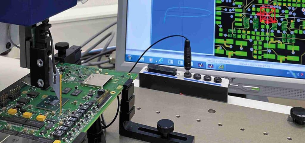
Figure 2. Pogo pins arranged to contact test pads on a PCB
Pogo pins allow easy connectivity for production testing but require additional upfront cost of fabrication custom spring-loaded connectors. They also take more board space than simple test pads.
Test Brackets and Ports
For some applications, direct test pad access is not feasible. Test brackets and docking ports serve as interfaces to route internal signals to an external test interface.
Docking test fixtures house probed pins that align and connect to landing pads on the PCB test port. The attached instrument can then access test points mapped to the dock probes.
Brackets may have pogo pins, edge connectors, or probing pins that secure to the PCB when testing is required. By disconnecting the test hardware from the main board, the system retains better integrity and noise isolation for normal operation.
Considerations for Placement of Test Points
Where test points are placed on the PCB layout makes a big difference in their accessibility and usefulness. Certain best practices help guide optimal test point positioning.
Accessibility
Accessibility should be the top priority when placing test points. They serve no purpose if probes cannot reach them! Avoid placing test points underneath large components or in obstructed areas without a clear probing path.
Ideally, test points group around related components that share debugging or calibration requirements. Board edges provide the most room for probing various angles. Placing at corners allows access from two sides.
Minimal Effect on Circuit
Care must be taken to isolate test nodes from the operation of high-speed or sensitive analog circuits. Long routing traces from the tapped node to the test pad can infringe on small signal paths or introduce interference and crosstalk issues. Stubs and vias may also degrade high frequency signals.
Test points should branch as close to the source node as possible through short direct routes. Vias are kept to minimum, avoiding 90 degree angles if possible. Guard rings around analog test point clusters help shield noise from digital circuits.
Clearly Labeled
The usefulness of well-placed test points gets eliminated if engineers spend extensive time figuring out the net each is connected to! Clear visible labeling with net names, designators, and voltages must appear next to all test points.
Silkscreen printing adjacent to the test pad is standard. For boards with many test points, a paper legend is often overlaid during testing to correlate locations with live readings.
Here is a summary of the key test point placement considerations:
| Consideration | Description |
|---|---|
| Accessibility | Allow easy probe access without components blocking |
| Small stubs | Minimize trace length to nodes |
| Little effect | Do not degrade signals with loading |
| Labeling | Print net names next to test pads |
Debugging and Testing Using Test Points
PCB test points serve several purposes during verification, debug, validation, and other production testing procedures.
Voltage Measurements
One of the most common applications is measuring local supply voltages and rail sequencing. Rather than needing to clip voltmeter leads at the power lugs, test points spaced around the board provide convenient monitoring nodes. Battery voltages, charge status, current draws can be quantified without disruption.
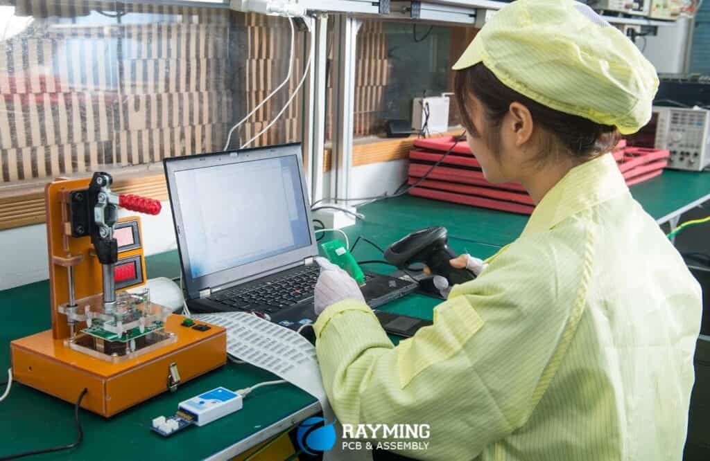
Figure 3. Example of technicians measuring test point voltages
Oscilloscope probes connected to ground provide differential readings that help trace unexpected voltage drops due to excessive loads or bad power connections.
Signal Injection
Test points allow input test signals to be injected into the circuit through appropriate buffering. Control logic can be pulsed to verify downstream response signaling. Clock or data stimuli applied to test nodes help characterize full system behavior when the source cannot be easily driven.
Function generators combined with probe measurement at other test locations facilitate system-level signal verification tests without specialized test equipment. Marginal timing faults can be detected by sweeping frequency ranges on the injected test stimulus.
Frequency Measurements
Oscilloscope probes attached to test points are the least intrusive way to monitor frequencies and edge timings of critical nets. High impedance 10X oscilloscope probes présent negligible loading to circuits when sized appropriately.
Frequency validity over voltage and temperature ensures robust operational margins. More advanced measurements like eye diagrams, jitter, phase noise characterize high frequency digital and clock networks.
Best Practices for Utilizing Test Points
Following certain guidelines and methods helps gain maximum utility from integrated test points during debug and validation.
- Define test plans early – Discuss test access requirements with designers when drafting board layouts. Trying to retrofit adds difficulty.
- Label all testpoints – Identify all test point names clearly on schematic and layout drawings.
- Provide external access – Bring groups of related test pads to a connector for easy attachment.
- Follow probing best practices – Use high impedance probes, distributed loading, calibrated equipment to prevent circuit disturbance.
- Develop test diagnostics – Create signatures, expected values and troubleshooting procedures for each grouped test node.
Well-planned test points following best practice recommendations should provide quality access, minimal invasiveness, and reliable information to accelerate the debug and verification process.
Conclusion
Test points satisfy a critical need for accessing internal PCB signals in a non-intrusive way during debug, validation, and troubleshooting stages of the electronics development cycle. Several test point solutions cater towards simplifying probing while isolating actual circuits.
Careful test point placement guidelines help engineers design high-quality test access without degrading operation. Labels, controlled impedances, and physical access considerations are weighed when planning board layouts. As increasing complex electronics necessitate controllability and observability for characterization, purpose-built test points continue to serve an indispensable role.
Frequently Asked Questions
What are some key benefits provided by PCB test points?
Some major benefits that test points enable:
- Non-intrusive debugging without affecting circuit operation
- Support for validation and production testing procedures
- Simplified diagnostics and field troubleshooting
- Risk mitigation from probing damage
- Design iteration with additional test points
What typical measurements are made using test points?
Common measurements involve:
- Voltage levels and power rail sequence validation
- Timing signal characteristics like clock frequencies
- Stimulus input signals injection to verify functionality
- Control logic pulse triggering to downstream logic pathways
How can test point access be made external for debugging?
Grouping critical nets’ test points along board edges allows connecting debugging hardware through:
- Edge pin header connectors
- Bracket connectors with pogo pins/probes
- Edge traces to wire leads
This grants easy external equipment attachment without affecting core board layout.
What is the difference between a via and plated through hole test point?
Vias are small holes that interconnect between layers while plated through holes span from top to bottom layer. Both can provide impromptu test access but via holes are too small for probes. For test points, larger through hole diameters (>20 mil) are recommended.
What labeling best practices should be followed for PCB testpoints?
Clear visually identifiable labeling helps easily identify test points:
- Place test point names on layout drawings/schematics
- Silkscreen print net names adjacent to test pad metal
- Create paper legends to affix near board under debug
- Follow consistent name conventions (EX: TP101, TP201 etc)


0 Comments