Introduction to PCB SMT Assembly
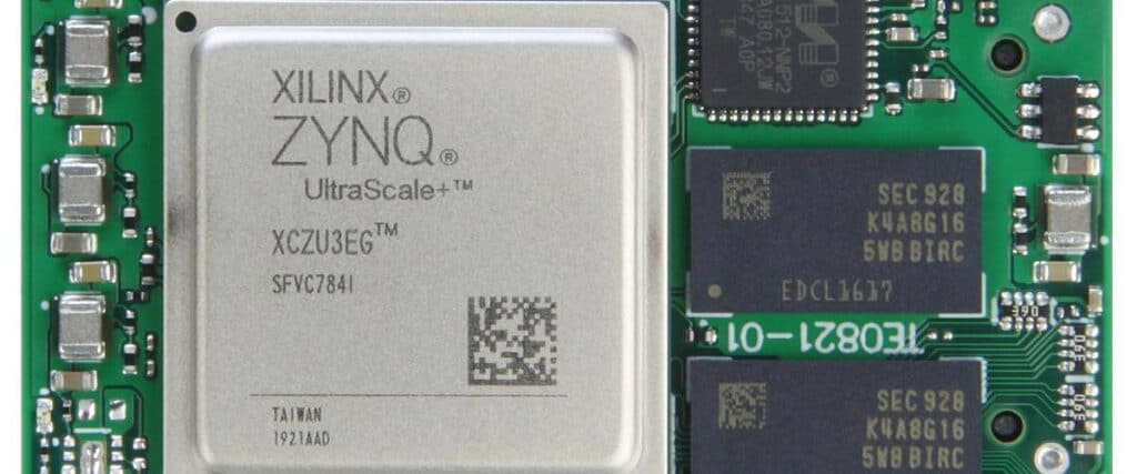
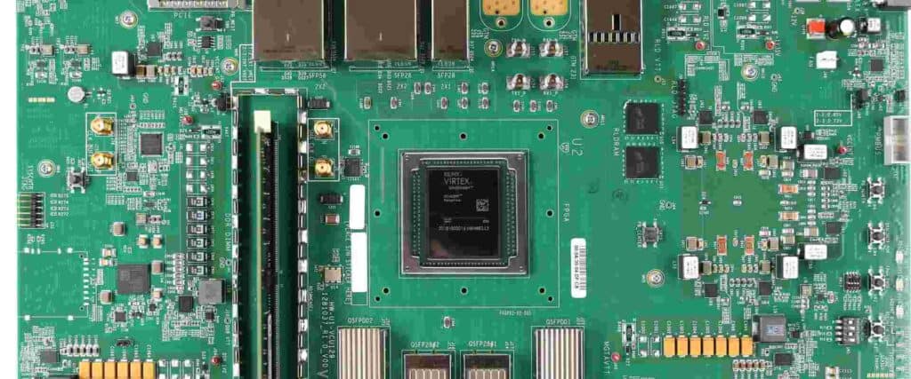
PCB assembly refers to the process of soldering electronic components onto a printed circuit board (PCB). SMT (Surface Mount Technology) is a method of assembling electronic circuits where the components are mounted directly onto the surface of PCBs without any wires or leads going through holes.
SMT has largely replaced the older through-hole technology and has several advantages:
- Smaller components allow for greater component density and miniaturization
- Automated assembly is easier
- Lower resistance and inductance allows higher speed signals
- Cost effective even at low volumes
- Both sides of the board can be used efficiently
The rest of this comprehensive guide will explore the SMT assembly process in detail.
SMT Assembly Process Step-by-Step
The typical SMT assembly process involves the following key steps:
1. SMT Stencil Design and Fabrication
- A stencil is a thin metal sheet laser cut with apertures matching the pads on the PCB.
- Solder paste is applied through the stencil onto PCB pads during printing.
- Accurate stencil design is crucial for defining solder deposit volumes.
- Stencils are typically made of stainless steel or nickel-plated brass.
2. Solder Paste Printing
- Solder paste contains solder metal alloy particles suspended in flux.
- An automated printer is used to align the stencil and print precise amounts of solder paste.
- Common printing methods:
- Screen printing: Squeegee spreads paste over stencil
- Jet printing: Solder droplets printed directly
- Aerosol printing: Solder sprayed through stencil
3. SMT Component Placement
- Robotic pick and place machines precisely position components on solder pads.
- Feeders supply components in reels, trays or sticks.
- Vision alignment systems check placement accuracy.
- Smaller ICs may use pin-in-paste or flip chip assembly.
<table> <tr><th>Component Size</th><th>Typical Accuracy</th></tr> <tr><td>Large (caps, connectors)</td><td>50-100 μm</td></tr> <tr><td>Medium (SOICs, QFPs)</td><td>25-50 μm</td></tr> <tr><td>Small (01005 chips)</td><td>10-25 μm </td></tr> </table>
4. Solder Reflow
- Reflow ovens melt solder paste deposits under controlled heating.
- Typical profile has preheat, reflow and cooling stages.
- Peak temperatures reach 230-260°C depending on alloy.
- The process solders all joints simultaneously.
5. Automated Optical Inspection
- Verifies all components are present with proper alignment.
- Checks for missing, misplaced or incorrectly oriented parts.
- Solder paste volume and fillet quality may also be inspected.
- Helps identify defects early to minimize rework.
6. Post SMT Cleaning
- Removes flux residue from assembly after soldering.
- Aqueous or solvent cleaning are typical methods.
- Ensures residue does not impact performance or reliability.
- May also involve rinsing, drying and baking steps.
7. Conformal Coating
- Protective polymer coating applied over the SMT assembly.
- Protects against environmental damage like moisture or dirt.
- Acrylic, silicone, urethane or epoxy coatings are common.
- Can be applied by spraying, brushing or dripping.
This completes a bare SMT PCB assembly. Additional processes like in-circuit testing or box build may then be performed according to product requirements.
SMT Assembly Equipment
Specialized equipment used for SMT assembly includes:
- Solder Paste Printers: Automatically print solder paste on PCBs.
- Pick and Place Machines: Robotically place components on boards.
- Reflow Ovens: Heat solder paste deposits to form joints.
- AOI Machines: Automated optical inspection.
- Cleaning Systems: Removes post-soldering flux residues.
- Conformal Coating Tools: Applies protective coatings.
High-quality equipment helps achieve reliable, high-yield SMT assembly. Leading equipment manufacturers include Panasonic, Yamaha, Juki, Mycronic, and Nordson among others.
Design for Manufacturing Guidelines
PCBs and component packages should be designed with SMT assembly in mind. Some design for manufacturing guidelines include:
- Prioritize two-sided board designs to maximize efficiency.
- Include generous tolerances for solder mask and pad sizes.
- Allow sufficient clearance around components and connectors.
- Use standard rectangular SMT packages where possible.
- Avoid odd component shapes or large pin counts.
- Design panels with multiple PCB arrays for batch assembly.
Following DFM principles ensures an optimized, high-quality assembly process.
SMT Assembly Challenges
Some potential challenges faced with SMT assembly include:
- Tombstoning: Partially lifted component due to incomplete wetting.
- Solder Balling/Flashing: Small solder balls form between pads.
- Solder Bridging: Solder forms unwanted bridge between pads.
- Voids: Trapped gas bubbles within solder joint.
- Warpage: PCBs warp due to thermal stresses.
- Head-in-Pillow: Flattened solder fillet shape.
- Icicles/Solder Webbing: Protruding spikes of solder.
Careful process control is needed to avoid these defects and produce reliable solder joints.
Advantages of SMT Assembly
Key benefits provided by SMT technology:
- Allows miniaturized and highly dense PCB assemblies.
- Automated assembly provides high throughput.
- Components are small, lightweight and low cost.
- Excellent electrical performance with solder joints.
- Reduces manual labor requirements significantly.
- Suitable for prototyping as well as high volume production.
- Flexible – wide range of component sizes accommodated.
SMT assembly provides significant size, performance, quality and cost advantages over traditional through-hole PCB assembly.
FQA
Why is SMT the preferred assembly method today?
SMT is preferred as it allows highly miniaturized and compact PCB assemblies. The small component sizes and automated assembly provide many cost and quality benefits as well.
What are some key SMT equipment used?
Key SMT assembly equipment includes solder paste printers, pick and place machines, reflow ovens, AOI systems and cleaning systems. High performance equipment is crucial.
How is solder paste applied during SMT assembly?
Solder paste containing metal alloy particles suspended in flux is applied by printing through a stencil onto the PCB pads. Stencil design matches the pads.
What is meant by pick and place in SMT assembly?
Pick and place machines use vacuum nozzles to pick components from reels and precisely place them onto PCB solder pads. Placement accuracy is critical.
What defects can occur with poor SMT process control?
Common SMT defects without proper process control include tombstoning, solder balls, solder bridging, voids, PCB warpage and others.


0 Comments