In the ever-evolving world of electronics, reverse engineering printed circuit boards (PCBs) has become an essential skill for hobbyists, researchers, and professionals alike. Whether you’re trying to repair an obsolete device, recreate a discontinued product, or gain a deeper understanding of existing technologies, reverse engineering PCBs can provide invaluable insights and opportunities.
This comprehensive guide will walk you through the process of reverse engineering PCBs, covering various techniques, tools, and best practices. From identifying components to deciphering circuit designs, we’ll explore the intricacies of this intricate process, enabling you to unlock the secrets hidden within the intricate layers of printed circuit boards.
Understanding Reverse Engineering
Before delving into the specifics of reverse engineering PCBs, it’s crucial to understand the concept and its applications.
Definition of Reverse Engineering
Reverse engineering is the process of analyzing an existing product or system to understand its design, construction, and operation. It involves systematically deconstructing and examining the components, materials, and principles that govern the product’s functionality.
Applications of Reverse Engineering PCBs
Reverse engineering PCBs has numerous applications across various domains, including:
- Repair and Maintenance: When dealing with obsolete or discontinued electronic devices, reverse engineering PCBs can help identify faulty components, understand circuit designs, and facilitate repairs or replacements.
- Recreating Legacy Products: In cases where original design documentation is unavailable or incomplete, reverse engineering PCBs can enable the recreation of legacy products or systems for historical preservation or continued use.
- Competitive Analysis: Reverse engineering PCBs can provide valuable insights into competitor’s products, allowing for comparative analysis, benchmarking, and identification of potential improvements or innovations.
- Educational and Research Purposes: Reverse engineering PCBs can serve as a powerful learning tool for students, hobbyists, and researchers, fostering a deeper understanding of electronic circuit design and functionality.
- Intellectual Property Analysis: In certain cases, reverse engineering PCBs may be necessary for intellectual property analysis, patent evaluation, or legal proceedings related to potential infringement or licensing disputes.
Preparing for Reverse Engineering
Before embarking on the reverse engineering process, it’s essential to gather the necessary tools and materials, as well as familiarize yourself with the PCB’s background information.
Obtaining the PCB
The first step in reverse engineering a PCB is to obtain the physical board itself. This could involve acquiring a working or non-working device, purchasing a spare PCB from a third-party supplier, or salvaging a board from an obsolete or discarded electronic product.
Gathering Background Information
Gather as much background information as possible about the PCB or the device it belongs to. This could include datasheets, schematics, user manuals, or any other documentation that may provide insights into the board’s functionality, components, or design.
Essential Tools and Materials
To effectively reverse engineer a PCB, you’ll need a range of tools and materials. Here are some essential items to have on hand:
- Magnifying glass or microscope
- Multimeter
- Logic probe or logic analyzer
- Desoldering tools (e.g., solder sucker, desoldering wick, hot air rework station)
- Soldering iron and solder
- Tweezers and precision tools
- Screwdrivers and pliers
- Chemical solutions for cleaning and etching (e.g., isopropyl alcohol, flux remover, ferric chloride)
- Protective equipment (e.g., safety glasses, gloves, masks)
- PCB design software (e.g., KiCad, Eagle, Altium Designer)
- Reference materials (e.g., component datasheets, application notes)
Reverse Engineering Process
The process of reverse engineering a PCB involves several stages, each building upon the previous one to unravel the intricacies of the circuit design.
Visual Inspection and Component Identification
Begin by carefully inspecting the PCB visually, taking note of any markings, labels, or identifying information on the components. Use a magnifying glass or microscope to examine the board closely, identifying components such as integrated circuits (ICs), resistors, capacitors, and other discrete components.
Reference datasheets, component markings, and online resources to identify the specific components and their functionalities. This step is crucial for understanding the board’s overall purpose and functionality.
Desoldering and Component Removal
In some cases, it may be necessary to desolder and remove components from the PCB to gain better access or to analyze them individually. Use desoldering tools and techniques carefully to avoid damaging the board or components.
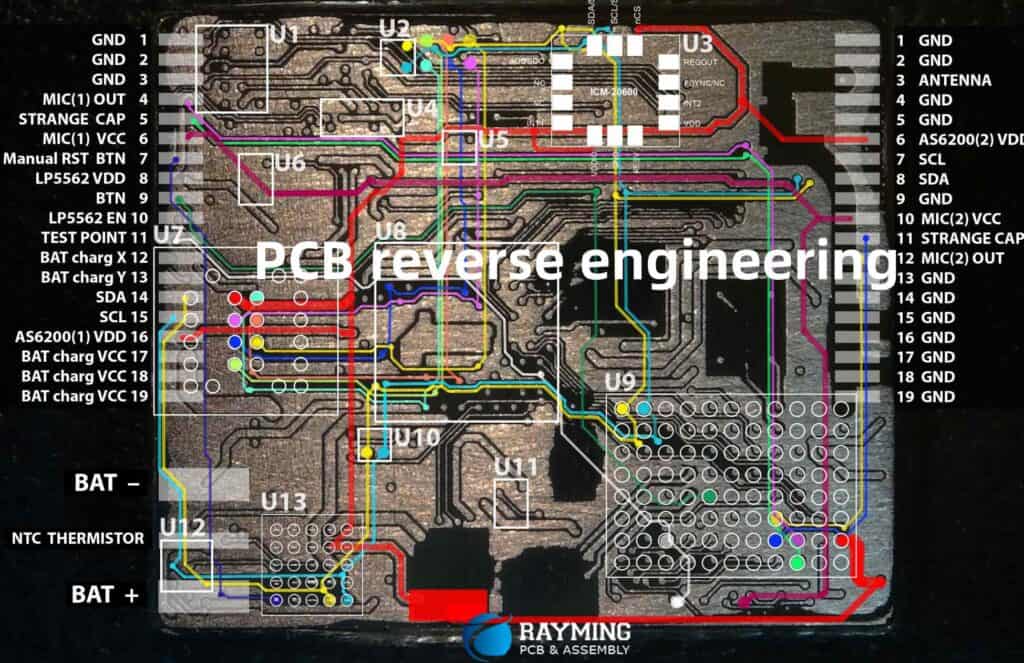
Circuit Tracing and Schematic Reconstruction
Once the components have been identified, the next step is to trace the interconnections and reconstruct the circuit schematic. This can be done manually by following the traces on the PCB or with the aid of specialized software that can generate schematics from PCB images or data.
During this process, pay close attention to the routing of traces, the placement of vias, and any specialized features or design considerations that may provide insights into the circuit’s functionality.
Signal Analysis and Circuit Verification
To further understand the circuit’s operation, it may be necessary to perform signal analysis and circuit verification. This can involve using logic probes, logic analyzers, or oscilloscopes to observe and analyze the signals present on the PCB.
By monitoring input and output signals, as well as tracking signal propagation through the circuit, you can gain valuable insights into the board’s behavior and verify your understanding of its functionality.
PCB Layout Analysis and Reverse Engineering
In addition to reconstructing the circuit schematic, it’s also essential to analyze the PCB layout itself. This includes studying the placement of components, the routing of traces, and any specific design considerations or constraints.
Understanding the PCB layout can reveal insights into signal integrity, electromagnetic compatibility (EMC), thermal management, and other critical aspects of the board’s design.
Documentation and Recreation
Once you have thoroughly analyzed and understood the PCB’s circuit design and layout, you can begin documenting your findings and, if desired, recreating the board. This may involve creating detailed schematics, PCB layout files, and documentation that captures the board’s functionality, specifications, and design considerations.
Recreating the PCB can be accomplished using PCB design software and appropriate manufacturing processes, allowing for the preservation, replication, or further study of the original design.
Best Practices and Considerations
Throughout the reverse engineering process, it’s essential to follow best practices and consider various factors to ensure accurate and reliable results.
Safety Considerations
Working with electronic components and chemicals can pose potential hazards. Always prioritize safety by using appropriate protective equipment, following proper handling procedures, and adhering to relevant safety guidelines.
Legal and Ethical Considerations
Reverse engineering PCBs may involve intellectual property rights, patents, or other legal considerations. It’s crucial to familiarize yourself with relevant laws and regulations, and to conduct reverse engineering activities within legal and ethical boundaries.
Documentation and Record-Keeping
Maintain detailed documentation and records throughout the reverse engineering process. This includes documenting component identifications, circuit schematics, PCB layouts, signal analyses, and any other relevant information or findings.
Collaboration and Knowledge Sharing
Reverse engineering can be a collaborative endeavor, especially when dealing with complex or specialized systems. Consider collaborating with experts, joining online communities, or participating in forums to share knowledge, seek advice, and contribute to the collective understanding of the subject.
Continuous Learning and Skill Development
Reverse engineering is a continuous learning process that requires ongoing skill development. Stay updated with emerging techniques, tools, and best practices by attending workshops, seminars, or seeking educational resources to enhance your knowledge and capabilities.
Potential Challenges and Limitations
While reverse engineering PCBs can be a rewarding and insightful process, it is not without its challenges and limitations. Here are some potential hurdles you may encounter:
- Component Identification Difficulties: Some components, especially integrated circuits (ICs) or specialized components, may be challenging to identify, requiring extensive research or specialized equipment.
- Trace Routing Complexities: In densely populated PCBs or multi-layer boards, tracing interconnections and reconstructing schematics can become increasingly complex and time-consuming.
- Signal Analysis Challenges: Analyzing signals and verifying circuit functionality may be hindered by factors such as signal degradation, noise, or the presence of specialized or proprietary protocols.
- Intellectual Property Restrictions: Reverse engineering activities may be restricted or prohibited in certain cases due to intellectual property rights, patents, or legal agreements.
- Documentation Limitations: In cases where original documentation or datasheets are unavailable, reverse engineering may be significantly more challenging or even impossible for certain components or systems.
- Time and Resource Constraints: Depending on the complexity of the PCB and the available resources, reverse engineering can be a time-consuming and resource-intensive process, requiring significant effort and dedication.
Table: Reverse Engineering Tools and Their Applications
| Tool | Application |
|---|---|
| Magnifying Glass or Microscope | Visual inspection and component identification |
| Multimeter | Measuring electrical parameters and verifying connections |
| Logic Probe or Logic Analyzer | Analyzing digital signals and logic levels |
| Desoldering Tools (Solder Sucker, Desoldering Wick, Hot Air Rework Station) | Removing components from the PCB for further analysis |
| Soldering Iron and Solder | Repairing or modifying connections on the PCB |
| Tweezers and Precision Tools | Handling and manipulating small components and traces |
| Chemical Solutions (Isopropyl Alcohol, Flux Remover, Ferric Chloride) | Cleaning, deoxidizing, and etching PCBs |
| PCB Design Software (KiCad, Eagle, Altium Designer) | Reconstructing schematics and PCB layouts |
| Reference Materials (Datasheets, Application Notes) | Identifying components and understanding their functionalities |
FAQ (Frequently Asked Questions)
- Q: Is reverse engineering PCBs legal? A: Reverse engineering PCBs can be legal, but it depends on the specific circumstances and the intended purpose. It’s important to familiarize yourself with relevant laws and regulations, as well as any intellectual property rights or legal agreements that may restrict reverse engineering activities.
- Q: How can I identify unknown components on a PCB? A: Identifying unknown components can be challenging, but there are several techniques you can employ, such as researching component markings, analyzing package types and pinouts, studying the component’s function within the circuit, and consulting online resources or datasheets.
- Q: What if I encounter multi-layer or high-density PCBs during reverse engineering? A: Multi-layer and high-density PCBs can be significantly more complex to reverse engineer due to the intricate routing of traces and interconnections. In such cases, you may need to employ advanced techniques, such as X-ray imaging or specialized software, to trace the interconnections accurately.
- Q: Can reverse engineering PCBs be used for competitive analysis or product benchmarking? A: Yes, reverse engineering PCBs can be a valuable tool for competitive analysis and product benchmarking. By understanding the design, components, and functionality of a competitor’s product, companies can identify areas for improvement, innovation, or potential patent infringement.
- Q: Is it possible to recreate a PCB design from reverse engineering? A: Yes, it is possible to recreate a PCB design from reverse engineering efforts. By reconstructing the schematic and PCB layout, and documenting the design considerations and specifications, you can use PCB design software and manufacturing processes to recreate the original board or develop a compatible alternative.
Conclusion
Reverse engineering printed circuit boards is a valuable and multifaceted skill that can unlock a wealth of opportunities in the world of electronics. From repairing legacy devices to gaining insights into cutting-edge technologies, the process of deconstructing and analyzing PCBs provides a unique perspective on the intricate designs that power our electronic systems.
By following the steps outlined in this guide, including visual inspection, component identification, circuit tracing, signal analysis, and PCB layout analysis, you can unravel the mysteries hidden within printed circuit boards. However, it’s essential to approach reverse engineering with a mindset of continuous learning, collaboration, and ethical consideration.
While reverse engineering PCBs presents its challenges, such as component identification difficulties, trace routing complexities, and potential intellectual property restrictions, the rewards of gaining a deep understanding of electronic circuit design and functionality make it a worthwhile endeavor.
As technology continues to evolve, the skills and knowledge gained through reverse engineering PCBs will become increasingly valuable, enabling you to navigate the complexities of modern electronics, contribute to innovation, and unlock new opportunities in various domains.


0 Comments