Introduction to PCB Assembly
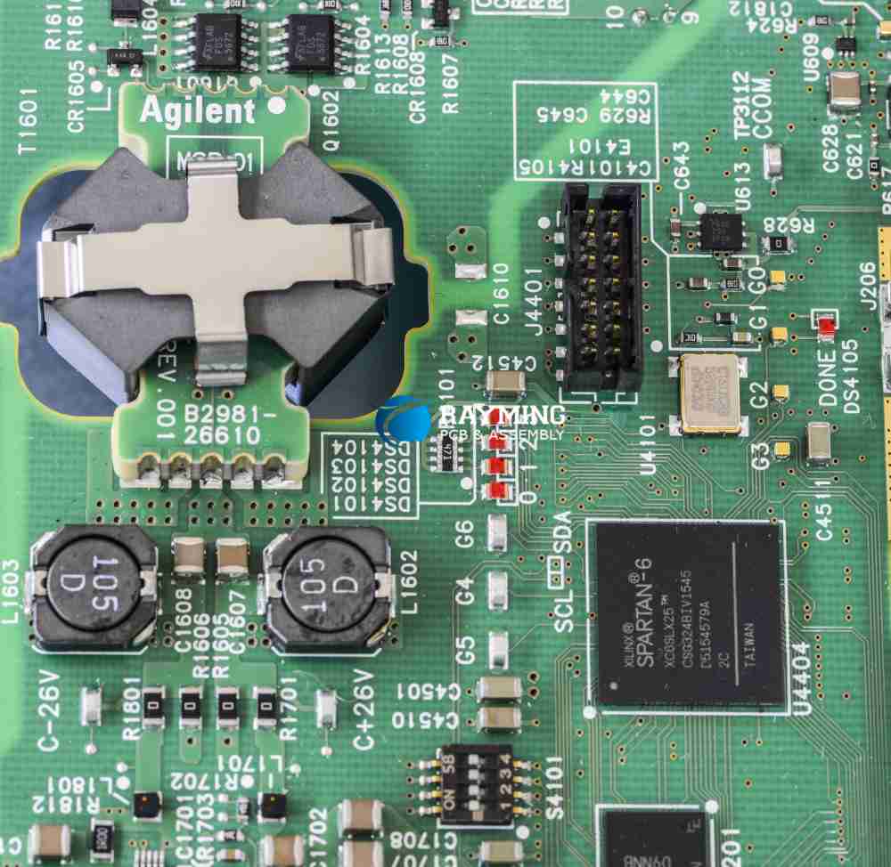
Printed circuit boards (PCBs) are essential components of most modern electronic devices. A PCB serves as the base for mounting and connecting electronic components using conductive copper traces etched from copper sheets laminated onto a non-conductive substrate. PCB assembly, also known as PCBA (printed circuit board assembly), is the process of soldering or assembling the components onto the PCB.
The PCB assembly process involves several steps:
- PCB design and fabrication
- Component procurement
- Solder paste application
- Pick and place
- Reflow soldering
- Testing and inspection
- Repair and rework
Proper PCB assembly requires expertise, precision tools, and quality control at each step. This article provides a comprehensive guide to PCB assembly, examining each step of the assembly process in detail.
PCB Design and Fabrication
The first step is designing and fabricating the printed circuit board itself. The PCB design must precisely specify the board’s dimensions, layer stackup, copper traces, and drill holes. Popular PCB design software packages include Altium, Cadence Allegro, and KiCad.
Once the PCB design files are ready, the board is fabricated by a PCB manufacturer. The fabrication process entails:
- Laminating copper foil onto the substrate, usually FR-4 fiberglass
- Coating the copper with photoresist
- Exposing the photoresist to light through the PCB design pattern
- Developing the photoresist to remove unexposed areas
- Etching away copper not protected by photoresist
- Drilling holes specified in the PCB design
- Plating the holes with copper
- Applying solder mask and silkscreen layer
- Scoring and breaking the board into individual PCBs
The fabricated blank PCBs are now ready for component assembly.
Component Procurement
The assembly process requires all the necessary components specified in the bill of materials (BOM). These electronic components include:
- Integrated circuits (ICs) – microcontrollers, memory chips
- Resistors, capacitors, inductors
- Transistors, diodes
- Connectors, switches, buttons
- Light emitting diodes (LEDs)
- Crystals, oscillators
- Any other active and passive surface mount or through-hole components required on the board
The procurement department must source these components at competitive pricing from authorized suppliers/distributors while meeting specifications, quality standards, and quantity requirements.
Solder Paste Application
Solder paste is first applied on the PCB pads to hold the components in place for soldering. The application methods include:
- Stencil printing – A metal stencil with cutouts matching the PCB footprint is aligned over the board. Solder paste is applied on top of the stencil and a squeegee blade spreads the paste through the stencil openings onto the PCB pads. This is the most common method.
- Dispensing – Solder paste is selectively deposited on pads through precision syringe tips or jetting valves. Used for applying paste on boards with a mix of surface mount and through-hole components.
- Printing – Solder paste is printed directly on pads using an inkjet-like print head. Provides the highest precision but lower throughput.
The composition of the solder paste includes solder alloy particles mixed with flux and stabilizing additives. Common solder alloys are SAC305 (Tin-Silver-Copper) and Sn63Pb37 (Tin-Lead). The stencil aperture design and solder paste properties must be optimized to apply the right amount of paste on each pad. Insufficient solder can cause defects like opens or tombstoning while excess solder can lead to bridging between pads.
Pick and Place
The pick and place machine accurately mounts the components onto their footprints on the PCB. This involves:
- Recognizing component and PCB fiducials for precise positioning
- Picking components from reels, trays, or sticks loaded by the operator
- Flipping/rotating parts oriented the right way up
- Placing components precisely on their pads with solder paste
- Pressing parts against the paste to temporarily adhere them
Pick and place machines utilize high-resolution cameras and nozzles with vacuum suction cups. Advanced systems use neural networks and computer vision for reliable component recognition. Pick and place constitutes the majority of the assembly time and requires programming the machine with the right positioning coordinates.
Reflow Soldering
With the components temporarily secured by solder paste, the PCB assembly undergoes reflow soldering. This melts the solder to form permanent electrical and mechanical joints between the pads and component leads.
Reflow ovens heat up the entire PCB assembly to melt the solder. Heating is done in different thermal zones – preheat, soak, reflow, and cool down. The peak temperature reached is above the melting point of the solder alloy used (usually 215-270°C). The reflow profile (time and temperature per zone) must be optimized to produce reliable solder joints without damaging components.
Other reflow methods include:
- Infrared/Convection oven – IR heaters above and convection fans below
- Vapor phase – Condensation of vaporized liquid perfluropolyether
- Laser – A laser beam scans over joints to heat them
- Induction – Electromagnetic induction heats the board locally
After reflow soldering, the board cools down with all components soldered securely. Visual inspection checks for any missing joins, unwanted bridging between pads, or disturbed components.
Testing and Inspection
PCB assembly testing validates the board’s functionality and detects any manufacturing defects:
- In-circuit test (ICT) applies voltage/signals to test points, checks continuity, and verifies the circuit works as intended through fixture-based testing.
- Flying probe uses movable test probes to contact test points on the board and runs functional testing.
- Automated optical inspection (AOI) examines the PCB under high-resolution cameras to check assembly quality – missing/misaligned components, poor solder joints, shorts, etc.
- X-Ray inspection sees through components and checks for hidden flaws in solder joints.
- Boundary scan tests interconnects between ICs with built-in boundary scan capability.
- Functional testing applies inputs to exercise the board in its intended application and validates overall functionality.
Any boards failing testing are repaired or reworked. The high number of tests ensures all assembled PCBs meet specifications.
Repair and Rework
Defects from the assembly process must be corrected:
Reassembly replaces damaged components using pick and place machine. Defective parts are removed by desoldering techniques like vacuum suction or heating.
Solder touch-up fixes insufficient solder joints by re-melting solder or adding fresh paste.
Solder wicking removes solder bridges by wicking away excess solder.
Pin straightening corrects bent component leads.
Conformal coating applies protective coating over the PCB assembly.
Reworked boards are re-tested before release. Only flawless boards proceed to delivery.
FQA
What are the key steps in PCB assembly?
The main steps in PCB assembly are:
- PCB design and fabrication
- Component procurement
- Solder paste application
- Pick and place assembly
- Reflow soldering
- Testing and inspection
- Repair and rework
Why is high precision required in PCB assembly?
Precision is critical in PCB assembly because components and copper pads are tightly spaced on the board. A minor alignment error of a few microns during placement or excess solder can cause short circuits between adjacent pads, rendering the board non-functional. Advanced PCB assembly tools like pick-and-place machines use high-resolution cameras, precision stages, and computer vision algorithms to achieve micron-level accuracy.
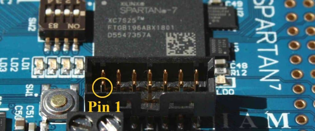
What is the difference between surface mount and through-hole components?
Surface mount components have leads/pads that directly sit on top of corresponding pads on the PCB surface. There are no holes, and the components are small in size. Through-hole components have long leads that are inserted into holes drilled in the PCB and soldered for both electrical and mechanical connection. Through-hole parts are larger and elevate above the board surface.
How does the stencil design affect solder paste application?
The metal stencil contains apertures that match the pad geometries on the PCB. The aperture dimensions like thickness, width and shape determine how much paste gets deposited on each pad. An optimal stencil design takes into account factors like pad size, pitch, component terminal geometry, and solder alloy to dispense the right amount of solder paste. Insufficient paste can cause defects from poor soldering, while excess paste increases the risk of solder bridging.
What is boundary scan testing?
Boundary scan testing uses built-in test circuitry mandated by the IEEE 1149.1 standard that is integrated into ICs. It provides access to pin interconnects to check continuity between IC pins after board assembly. Boundary scan helps detect soldering faults like open circuits and shorts without using physical test probes.
Conclusion
PCB assembly is a complex, multi-step manufacturing process requiring expertise, precise tools, quality materials, and rigorous testing. Each step from PCB fabrication, solder paste deposition, component placement to reflow soldering must be done with utmost accuracy and repeatability. PCB assembly plays a critical role in transforming bare boards into fully functional electronic devices and systems. As products become more compact with shrinking feature sizes, the demands on assembly quality continue to increase.


0 Comments